Friday, November 22, 2013
LM1800 FM Stereo Demodulator
This FM Stereo Demodulator circuit that use phased lock loop techniques to regenerate the 38kHz subcarrier is designed using the LM1800 integrated circuit .The LM1800 integrated FM stereo demodulator has numerous features like :automatic stereo/monaural switching , 45 dB power supply rejection ,wide operating supply voltage range ,excellent channel separation .As you can see in the circuit diagram this lm1800 fm stereo demodulator has a 100mA stereo indicator lamp driver.
LM1800 FM Stereo Demodulator Circuit diagram
LM1800 FM Stereo Demodulator Circuit diagram

For this LM1800 Phase-Locked Loop FM Stereo Demodulator circuit , you will need an dc power supply that can provide an output voltage between 10 and 18 volts .Also if you can not find the LM1800 Phase-Locked Loop FM Stereo Demodulator circuit on the market you can use the UA758 ic which is pin-to-pin compatible with LM1800 .
Amplifier Circuit with IC AN7143
On this Integrated circuit power amplifier use IC AN7143 but you can use this following IC :
| AN7147 | HA1377 |
| AN7149N | HA1377A |
| AN7168 | HA1392 |
| AN7169 | HA1398 |
| AN7176 | HA13102 |
| AN7178 | HA13108 |
| M5160L | ULX3777 |
You can use all the IC above on this circuit below :

This Circuit require minimum voltage 9 volt , and Maximum voltage 24 volt. Supply voltage with dual voltage not triple voltage. Maximum Output power 2 X 20 watt , with minimum impedance 4 Ohm. This is a stereo power amplifier Circuit. Notif the similiar IC have each distinct power.
Thursday, November 21, 2013
USB Car Charger Adapter
This USB car charger adapter project is a DC DC power converter that safely converts the 12V car battery voltage into stable 5V. This USB car charger circuit can be used to supply power from a car cigar lighter socket to a portable device that require a 5 volts . This circuit makes it possible to power/recharge any USB power-operated device, using in-dash board cigar lighter socket of your car.
USB Car Charger Adapter Circuit diagram

The DC supply available from the cigar lighter socket is fed to an adjustable, three-pin regulator LM317L (IC1). R1 and R2 resistors regulate the output of IC1 to steady 5V, which is available at the ‘A’ type female USB socket. Red LED1 indicates the output status and zener diode ZD1 acts as a protector against high voltage.As you can see in the circuit diagram , the circuit is very simple and require just few common cheap components .Because this circuit not require many components , you can put all components in the cigar plug socket .
USB Car Charger Adapter Circuit diagram
The DC supply available from the cigar lighter socket is fed to an adjustable, three-pin regulator LM317L (IC1). R1 and R2 resistors regulate the output of IC1 to steady 5V, which is available at the ‘A’ type female USB socket. Red LED1 indicates the output status and zener diode ZD1 acts as a protector against high voltage.As you can see in the circuit diagram , the circuit is very simple and require just few common cheap components .Because this circuit not require many components , you can put all components in the cigar plug socket .
450W audio power amplifier circuit
 Below it is a circuit of power amplifiers with power output of 450 watts mono , amplifiers are also frequently used in the amplifier a high-power amplifier, which used in an event, in the field and the placed closed. Because this amplifier suitable for the woofer, fullrange speaker, and can also be fixed for the subwoofer speaker.
 To further strengthen and maximize the amplifier ,its power supply circuit also must be accurate, for electrolytic capacitors in power supply ,voltage capacitors use 80V or more, and a capcity 20000uF upwards, so when the bass amplifier is high , the voltage is not lot of experience dropping. Diode bridge use a minimum of 35A, or adjust the current input voltage. If the power supply has fulfilled the desire, the supply to the power amplifier.

Schematic Audio Power Amplifier with IC AN7110 AN7130
Description Schematic :
Minimum Voltage for this Circuit is 6 Volt , and Maximum voltage is 18 Volt . To recomended circuit working use voltage 12 Volt. Its not So much and less , its good. Output speaker is Mono with power 1,2 watt and Impedance 8 Ohm. IC equal with AN7130.
See schematic circuit audio power amplifier AN7110 or AN7111 :
 |
| Click to view Enlarge |
Wednesday, November 20, 2013
Rapid battery charger schematic
The First ac voltage from tranformator will be rectified and filtered to the LM723 voltage regulator and the NPN pass transistors setup for constant current supply. The 470 Ohm resistor is limit trickle current the momentary pushbutton (S2) is depressed, the SCR turn on , and the current flows through previously determined resistor network.SCR will be turn off if thermal cutout inside the battery pack opens up.

Read More..
Digital Radar Speedometer Schematic
This circuit is a Digital Radar Speedometer. It allows us to evaluate the speed of any object moving, especially cars and other vehicles. The speed is calculated in kilometers per hour (KPH). Its display has three digits. This radar works with the laser reflexion. It sends laser radiation to the object and this object reflects the laser radiation to the radar. To evaluate the speed of a vehicle, we must be in front of it. In other words, the vehicle must come in our direction. The front of the radar must point the front of the vehicle. The radar has the shape of a pistol. In this radar, it has a laser LED and a laser diode. Both have a lens.
Digital Radar Speedometer Circuit Diagram

The laser LED can send a spot of light to a distance of 90 m (295 ft). Its very important that the distance range of the laser LED is 90 m, if not, the speed will not be calculated properly. The laser diode, which receives the light signal by the laser LED, must be able to detect the light which is same color as that emitted by the laser LED. The laser diode and the laser LED must be placed one beside the other. They are protected by a tinted pane. They must be placed at the front of the radar and point the outside. The radar is powered by a 9V battery and it has a SPST switch to control its power state.
The display, or the speed indicator, is placed at the rear of the radar, just on the right of the overload LED indicator. All the logic components of the circuit must be of the 74AS series and TTL type. Because they have short time of response (less than 1.7 ns) and have high frequency supports (more than 200 MHz). The radar can evaluate the speed of an object moving between 0 to 999 km/h. After this speed, the overload LED indicator will turn on and the "999" will still displayed. The radar displays the speed during 3 seconds, after this time, it displays "zero" (0).
Digital Radar Speedometer Circuit Diagram
The display, or the speed indicator, is placed at the rear of the radar, just on the right of the overload LED indicator. All the logic components of the circuit must be of the 74AS series and TTL type. Because they have short time of response (less than 1.7 ns) and have high frequency supports (more than 200 MHz). The radar can evaluate the speed of an object moving between 0 to 999 km/h. After this speed, the overload LED indicator will turn on and the "999" will still displayed. The radar displays the speed during 3 seconds, after this time, it displays "zero" (0).
Power Supply with regulation
 Electronic devices should be powered by direct current supply of DC (direct current) which is stable in order to work properly. The battery or batteries are the source DC power supply is best. However, for applications that require power supplies larger, the source of the battery is not enough.
A major source of power supply is alternating source of AC (alternating current) from power plants. For that needed a power supply device that can convert AC current into DC. In this article presented the principles of the power supply circuit (power supply), linear start from the simplest rectifier circuit to the power supply was regulation.
Power supply is functioning electronic circuit to supply power to other components in perangakat electronics. All electronic components that exist in an electronic device will receive power supply from the power supply. Power supply is very has a very important role in an electronic device. Therefore, without power supply, an electronic device will not work. The common voltage supplied by the power supply is +5 V, +12 V,-5V,-12V.
Large output voltage of power supply also must we adjust the voltage needs burden or our electronic devices. Because, an electronic device will be able to work well if the supply voltage and power to him just like the specifications of these electronic components. (specification can be seen in the datasheet of a component).

Power supply circuit drawing examples above we can replace with our needs. Pictured above is a simple power supply circuit having 78XX LM as a regulator. Type LM 78XX can we replace it according to our needs. If for example we want the output from the power supply is +12 Volts, then we have to change it into LM7812 LM. And also of course we have to input voltage of +12 volt transformer.
Similarly, if we want a voltage of +5 volts. So we have to replace the LM7805 LM 78XX, and the input voltage from the transformer 5Volt (transformer).
Tuesday, November 19, 2013
6 Watt 4 Ohm Amplifier Circuit
This is an audio amplifier circuit based on IC, and IC were used that MPC563 with minimal output 6W, with impedance of 4 Ohm. Supply Voltage Minimum 4 Volt DC and a maximum voltage to 20 Volts DC. See him under this Scheme.
 |
| 6 Watt 4 Ohm Amplifier Circuit |
AC to DC 90 Watt Switching Adaptor
 AC to DC 90 Watt Switching Adaptor Circuit
AC to DC switching adaptor circuit with best achievement ability of 90W. Switching ability accumulation is congenital application a aerial voltage ability switching regulator IC MC33374 and some added added components. The MC33374 IC is a caked aerial voltage ability switching regulators that are distinctively advised to accomplish anon from a rectified AC band source, and in flyback advocate applications.
The MC33374 switching ability adaptor combines the appropriate advocate functions with a different programmable accompaniment controller. At assorted capricious AC inputs, it is able of confined up to 6 A accepted at 15V achievement voltage. This switching ability adaptor is able of accouterment an achievement ability in balance of 150W with a anchored AC ascribe of 100V, 115V, or 230V, and in balance of 90 W with a capricious AC ascribe that ranges
4A High Speed Low Side Gate Driver
The UCC27518 and UCC27519 single-channel, high-speed, low-side gate driver device is capable of effectively driving MOSFET and IGBT power switches. Using a design that inherently minimizes shoot-through current, UCC27518 and UCC27519 are capable of sourcing and sinking high, peak-current pulses into capacitive loads offering rail-to-rail drive capability and extremely small propagation delay typically 17 ns.
The UCC27518 and UCC27519 provide 4-A source, 4-A sink (symmetrical drive) peak-drive current capability at VDD = 12 V. The UCC27518 and UCC27519 are designed to operate over a wide VDD range of 4.5 V to 18 V and wide temperature range of -40°C to 140°C. Internal Under Voltage Lockout (UVLO) circuitry on VDD pin holds output low outside VDD operating range.
4A High-Speed Low-Side Gate Driver Circuit diagram:

Features:
Device Uses:
The UCC27518 and UCC27519 provide 4-A source, 4-A sink (symmetrical drive) peak-drive current capability at VDD = 12 V. The UCC27518 and UCC27519 are designed to operate over a wide VDD range of 4.5 V to 18 V and wide temperature range of -40°C to 140°C. Internal Under Voltage Lockout (UVLO) circuitry on VDD pin holds output low outside VDD operating range.
4A High-Speed Low-Side Gate Driver Circuit diagram:
Features:
- Low-Cost, Gate-Driver Device Offering Superior Replacement of NPN and PNP Discrete Solutions
- Pin-to-Pin Compatible With TI’s TPS2828 and the TPS2829
- 4-A Peak Source and 4-A Peak Sink Symmetrical Drive
- Fast Propagation Delays (17-ns typical)
- Fast Rise and Fall Times (8-ns and 7-ns typical)
- 4.5-V to 18-V Single Supply Range
- Outputs Held Low During VDD UVLO (ensures glitch free operation at power-up and power-down)
- CMOS Input Logic Threshold (function of supply voltage with hysteresis)
- Hysteretic Logic Thresholds for High Noise Immunity
- EN Pin for Enable Function (allowed to be no connect)
- Output Held Low when Input Pins are Floating
- Input Pin Absolute Maximum Voltage Levels Not Restricted by VDD Pin Bias Supply Voltage
- Operating Temperature Range of -40°C to 140°C
- 5-Pin DBV Package (SOT-23)
Device Uses:
- Switch-Mode Power Supplies
- DC-to-DC Converters
- Companion Gate Driver Devices for Digital Power Controllers
- Solar Power, Motor Control, UPS
- Gate Driver for Emerging Wide Band-Gap Power Devices (such as GaN)
Monday, November 18, 2013
100 watts Symasym5 Power Amplifier
Symasym5, is a "cute" power amplifier, designed with quality but still low price in mind. This resulted in a ClassAB BJT amplifier, using only TO92 transistors for input and VAS, with a reasonable part count. The topology used is well known and consist of a single diffamp for input, plus a 2nd diffamp with current mirror for VAS. This is followed by normal darlington EF outputstage using modern high beta devices. The circuit uses large amounts of feedback over the whole audioband and an unconventional feedback compensation scheme. Right now symasym is designed to be driven directly from a CD/DVD-player, simply place a 22k poslog stereo pot between player and symasym. (as voltage divider)
Update
The at least change is to reduce C14 from 22pF to 10pF, but i recommend to follow Pavels advice. I recommend C14 with 10pF also for MJLs, this increases safety margin. Do not forget to read Pavels Review! A very promising evaluation of the qualities to be expected from symasym. Thanks Pavel ! Another update are the resistors R31/32 to be increased from 22ohm to 47ohm.
Symasym5_3 is an update of v5.2, with an improved board layout concerning power gnd, resulting in lower thd for high frequencies, giving more clarity in sound. The Page for symasym5_2 still exists.
If the gain is too high because symasym is driven from preamp, R30 can be increased from 499ohms to 1k, but in this case R16/19 (22 or 33 ohms, not on schematic, REs to Q1/2) are required to keep feedback at same level and
 |
| 100 watts Symasym5 Power Amplifier |
Some Specs :
- THD: ~0.005% (measured) simd: 0.002%
- Power into 8ohm: 60 watts
- Power into 4ohm: 100 watts
- Gain: 32dB (~1:40) full output at 0.7v input (0.5v rms)
- Feedback: 57dB
- GainBandWidth: ~400Mhz
- Slewrate: ~20v/us (symetrical)
- Supply voltage: +/- 36v
- Biasing: 55ma, ~12mv across a single 0.22 ohm
- Measurings: RMAA Symasym5 The measuring setup itself is far from perfect, but gives a good idea !
- Frequency response: 3.2hz to 145khz (-1db) using 4.7uf input cap
- Phaseshift at 10khz: <3°
- More will follow !
Schematic
Subwoofer amplifier schematic diagram
Amplifier circuit is very suitable for use in subwoofer speaker, because its strong. This circuit using ic, ic based on STK. to use it can be used on cars that use speakers or a subwoofer system in his car. 30 V supply voltage that has been rectified. Power output 20W mono.

Part List :
R1 = 100K
R2 = 47R
R3 = 100R
R4 = 1R
C1 = 220uF
C2 = 100uF
C3 = 100uF
C5 = 10uF
C6 = 1uF
C7 = 1uF
C8 = 1000uF
C9 = 0.1uF
IC = STK011 , STK015 , STK016
Sunday, November 17, 2013
Series electric circuit
Series electrical circuit is an electrical circuit, in which the input of a component derived from the output of other components. This has led to a series electrical circuit can save costs (fewer connecting cables used). In addition to own excess, a series electrical circuit also has a weakness, if one component is removed or damaged, then the other components will not function properly. Eg light bulbs strung together three series, the input of a single lamp light output will come from the other. If one lamp removed or damaged, then the other lights will go off. Consider the following series of three lights :
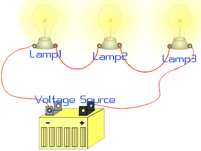 |
| Series electric circuit of three lights. |
Replacement series resistance equation can be sought from the initial equation, in which a strong electric current on each of each hambaran is the same, while the potential difference across each distinct value of each barrier.
0 4W power amplifier with 5G37 IC
This circuit requires a voltage of 6-12 Volts. To have a good quality of this series with the voltage necessary suplly good too. The definition of good that is filtered and does not release much ripple voltage and using large-capacity condenser elco issued for the bass is strong enough.
See below this circuit :

Datasheet IC 5G31A
Vcc = 6-12 V
Pout = 0,4 W
RL = 8 Ohm
Ft = 40-17 Khz
Icco = 15 mA
Package = TABS1-14
Manufactered = China
Saturday, November 16, 2013
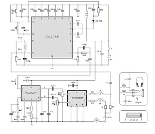
Stereophonic circuit with TDA7088T
There are two signals that are directed at the so-called FM transmitter the coder (coding). Multiplexing Mpx signal has been contained, two left signals and right indirectly. Frequency modulation of a transmitter carried by the signal Mpx. The receiver output signal is obtained on Mpx and FM detector is then passed to the decoder. At the decoder do the opposite with the coder in the transmitter, because at this level produced two signals L and D.
Signal is amplified by audio amplifier dientik two, then reproduced through two speakers are the same. Now listeners can heard coming from the left half the loudspeaker is placed on the left and right half of which is placed on the right side. Situation amid the orchestra will be equal to that of the second lordspeaker reproduced, made an impression on the listener as if there.
The third loudspeaker placed midway between the left and right. Based on all these listeners have a picture of the layout space, which is significantly increased total musical impression. Electronic circuits of the portable stereophonic radio receiver with headphones reproduction, made by the IC TDA 7088T is shown in Figure the above. This is a practical embodiment of the receiver with TDA7040T decoder and two audio amplifier with TDA7050T IC.
Choke (coils) L3, L4 and L5 are HF coil allows the headphone cable is used as a receiving antenna. this fulfilled by connecting one contact of the plug-in headphones, through a 10 pF capacitor at the point where the output of the antenna is connected. Coil has a significant barrier to the signal station, preventing ground connection through capacitor 47 mF or through the TDA7050T output.
LTC2990 System Monitoring IC
Using LTC2990 integrated circuit you can design a very simple monitoring system to monitor system temperatures, voltages and currents. Through the I2C serial interface, the device can be configured to measure many combinations of internal temperature, remote temperature, remote voltage, remote current and internal VCC. The internal 10ppm/°C reference minimizes the number of supporting components and area required. Selectable address and configurable functionality give the LTC2990 flexibility to be incorporated in various systems needing temperature, voltage or current data.
Bellow you can see some ideas how to use the LTC2990 I2C Temperature, Voltage and Current Monitor Ic in your electronic projects .
You can use LTC2900 IC for electronic projects like :motor protection , fan temperature alarm , battery monitoring , liquid level sensing and many other projects .
Bellow you can see some ideas how to use the LTC2990 I2C Temperature, Voltage and Current Monitor Ic in your electronic projects .
You can use LTC2900 IC for electronic projects like :motor protection , fan temperature alarm , battery monitoring , liquid level sensing and many other projects .


Basic Low Pass Filter

Low pass filter is a low-pass filter with low frequency signals but attenuates (reduces the amplitude of) signals with frequencies higher than cutoff frequency. The actual amount of damping for each frequency varies from filter to Filtering.
Sometimes called-high-cut filter, or treble cut filter when used in audio applications. Low-low pass filter is the opposite of the band-pass filter.
Sometimes called-high-cut filter, or treble cut filter when used in audio applications. Low-low pass filter is the opposite of the band-pass filter.
 |
| Low Pass Filter Basic Circuit |
The concept of low-pass filter exists in many forms, including electronic circuits (like a hiss filter used in audio), digital algorithms for smoothing data sets, acoustic barriers, blurring the image, and so forth.
Friday, November 15, 2013
Power Supply no transformer using IC and MOSFET

Pulsating DC voltage from rectifier D1 - D4 has a peak value 310 V This voltage is supplied to the spout of the power MOSFET T1 through a resistor divider R9. A control circuit ensures MOSFET will only deliver a short dive before and after the voltage through zero meshes. During this time do not go too far pulsating DC voltage 5 V. In a short time the same grading Capacitor C2 will be too fit, long time thereafter he gives the output current. Capacitor result should be worth a very large 10,000 μF. Load current pulses in a short time has a price peak in the 4th order A!
 |
| Schematics MOSFET use BUZ74 and IC CA3130E |
Output voltage stability essentially depends on the load. Maximum output current can be 110 mA. Supply for control circuit is obtained from the resistor R2., Capacitor C1 and the diodes D5 and D6. Control circuit is formed penanding window of three op-amp. The correct calibration of the controlling circuit becomes very important. Before the nets are given, first set the P1 in the middle position and turn the S2 until penggesernya are on earth potential. Then connect the nets and inspect the working voltage range. Next connect a voltmeter (10V DC range) on the output and adjust P2 until the meter begins to deviate. Finally, set P1 for meter reading 4.8 - 5 V.
Use of this circuit is limited. Obviously, can not be used with equipment that must be electrically insulated by the nets. It is also equally good when used with equipment which is very sensitive to sigh and nails nets. But good enough for the equipment that is not enough place to net transformer. This unit should be used to power the equipment that was placed in a plastic container. Any equipment that is powered by this circuit should not be connected to other equipment via a cable. If required to do must be done through optical coupling only.
The amount of heat dissipation at T1 and R9 only around 3 W. So if this rangkian installed in small contacts, there would be no problem with the heat. During the assembly, carefully observe first-prevention precautions are necessary in connection with a circuit that works with the nets.
Warning! This circuit needs to be made with extreme caution, because the nets full voltage there at some point.
IR Remote Control Extender Mark 5
The latest addition to my collection of Infra Red (IR) Repeater circuits. The Mark 5 is a much improved version of the Mark 1 circuit and has increased range and sensitivity. It is also immune to the effects ofambient light, daylight and other forms of interference. In addition it works with IR modulation freuencies in the range 30 to 120kHz making the Mk5 circuit the best choice for compatibility with remote controls.

Parts List:
R1,R2: 5M6 RESISTOR (2)
R3,R5: 3k3 RESISTOR (2)
R4: 120k RESISTOR (1)
R6: 220R RESISTOR (1)
R7: 47k RESISTOR (1)
R8: 120R RESISTOR (1)
R9: 10k RESISTOR (1)
R10: 2K2 RESISTOR (1)
R11: 100R RESISTOR 1 W (1)
C1,C3,C4: 22n polyester CAP (3)
C2: 100u electrolytic 25V(1)
C5: 100u electrolytic 25V(1)
Q1 BC107 (1) alternatives, BC107A, 2N2222, 2N2222A
Q2 BC109C (1) alternatives, BC109, BC549
D1: 1N4148 DIODE (1)
D2: Red LED (1)
IC1,IC2 CA3140E opamp (1)
IR1: SFH2030: (1)
IR2,3: TIL38 (2) or similar.
Design Philosophy:
This time I have returned to "first principles" and built a wideband infra red (IR) preamp which receives and re-transmits the entire baseband signal from a remote control handset.
It is designed to work with IR controls using 30-120KHz and should therefore work with just about any handset. In addition I have separated ambient (surrounding) light from the modulated light used by a remote handset. The major problem with the Mark 1 circuit is that it reacts to all light sources, ambient light producing a continous signal from the IR photo diode and is amplified by the rest of the circuit. I have published a modification to the original Mark 1 circuit, click here to view.
Noise Immunity:
It is difficult working with Infra Red, you cannot see it, and it is difficult to measure. A major barrier with this circuit was how to differentiate between daylight and an IR signal. Ambient light produces an almost continuous signal, changing little over several hours. A signal from an IR handset contains control pulses modulated with a carrier frequency (typically 36kHz) transmitted using an Infra Red photo diode. My solution used here, is a simple RC filter formed by C1 and R3.
At low frequency i.e. 50Hz the impedance of C1 is high, around 144k. The voltage gain of inverting op-amp IC2 is approximately R4 / R3, but at low frequency C1 is in series with R3 so the gain is now 120k / (3.3k + 144k) or less than unity. Daylight or ambient light will change slowly over several hours, in frequency terms this signal would be millihertz or less and C1s impedance will be megaohms.
A signal from an IR handset will be modulated at around 36KHz. At this frequency the impedance of C1 is very low, around 200 ohms. This has little effect on the input impedance of the op-amp stage and voltage gain will now be R4 / R3 or about 34 times. The impedance of capacitor C4 also helps noise rejection as its impedance change will allow more signal to pass into Q1 base at high frequencies and much less signal at line frequencies.
Circuit Details:
Light photons are received at IR1, this is an IR photo diode type SFH2030. A SFH2030F, which contains a daylight filter,may also be used instead of the SFH2030. The photo diode is reverse biased and when light strikes it, the energy of the IR signal releases additional charge carriers within the diode, allowing more current to flow. This current is amplified and converted to a voltage by the first CA3140 opamp, IC1. IC1 is wired as a current to voltage convertor, see below.

In an ideal current to voltage convertor the output voltage would be the product Rf multiplied by the input current. The non-inverting input would be tied to ground. In the Mark 5 circuit the output voltage is iR1 or about 5.6 Volts/uA appearing at pin 6 of IC1. The current generated by the SFH2030 photo diode when receiving a signal from a handset several metres away is less than 50 nA and requires the extreme high input impedance to avoid shunting the signal. There are two reasons for using the CA3140, the first is its high input impedance, over 1000G. The second reason is that normally the non-inverting input would be at 0V when working from split + and - supplies. In this single supply version the non-inverting input is returned to negative supply via R2. This can only be done with a Mosfet input, hence the choice for using the CA3140.
IC1 converta all current from the photo diode IR1 into a voltage. Although the SFH2030 is most sensitive at infra red wavelengths, it will produce tiny currents from daylight and also the 50/60Hz noise fields from flourescent and mains lighting. To minimize this, C1 and R3 form a high pass filter, allowing a 30kHz and higher signals to pass but blocking low frequencies. The impedance of C1 increases with decreasing frequency being 31k at 50Hz. Daylight for example, produces a contstant luminence, changing slowly over several hours, to which the impedance of C1 is effectively infinite.
The signal voltage from IC1 is now further amplified by IC2, gain being the ratio R4/R3 or 31dB. All opamps have a limit called the gain bandwidth product. The gain will fall to unity at the highest usuable frequency and be a maximum value at dc. Between these limits the gain falls with increasing frequency as shown in the bode plot for the CA3140 below:

Looking at the chart above, at 100kHz the maximum gain can only be about 30dB. However this is ample and boosts the received range of signals from a remote handset to the photo diode which have worked well up to 4 metres apart. Because R5 is returned to the negative supply a Mosfet input opamp must again be used. The output is again filtered by a high pass filter comprising C4 and the associated input impedance of Q1. R6, C2 and C3 provide decoupling for the IR preamplifier, C3 is in parallel with C2 because an electrolytic is not always a low impedance at high frequencies.
The IR output stage is comprised of Q1 and Q2 and associated components. The output is arranged so that with no input signal, Q1 is on and Q2 off; the visible LED, D2 will also be off. With no signal the 47k resistor biases the driver transistor, Q1 into full conduction. Its collector voltage will be near zero volts and the output transistor Q2, which is direct coupled to Q1 collector will therefore be fully off. Power drain will be minimal.
When an IR signal is receieved from a handset, the complete modulated signal will be amplified and fed via C4 into Q1 base. This is sufficiently strong enough to overcome the positive bias supplied by R7 and switch off Q1. This will happen many times a second, at the same frequency as the IR modulating signal sent by the handset. As Q1 switches off, its collector voltage rises to near full supply switching on Q1 and lighting the LED D2. Pulses of infra red at the same modulating frequency are then transmitted by the photo emitting diodes, IR2 and IR3. Because the signal is cleaner, (i.e. no daylight or 50/60Hz lamp fields included) then the series resistor R11 has been incresed in value to 100 ohms. The range from photo emitter diode to the equipment to be controlled has proved successfull at over 4 metres when powered from a 12 Volt supply. D1 helps to improve the turn off speed of Q1, thereby ensuring that the output waveform will be "squarer". It can be omitted but the circuit will perform better if D1 is included. A simulated transfer characteristic is shown below:
AC Transfer Charcteristic

The ouput is measured between Q2 emitter and ground. A simulated transient response is shown below. Three graphs are produced with excitations of 40,80 and 120kHz.

Please note that the above waveforms are simulated using a perfect square wave input, with rise and fall times of zero seconds. The output is measured between Q2 emitter and ground with a 200 ohm resistive load. In the real world, the cable to the remote photo emitter LEDs will contain both capacitance and inductance. This will increase both rise and fall times of the output signal. As with the Mark 1 circuit I recommend using speaker wire or bell wire to be used to cable the remote photo emitters.
My Prototype
Note that the veroboard layout below only includes the componets from the left of the schematic to C4, I had Q1 and Q2 on breadboard during this testing phase.

Setup and Testing:
There is little to adjust in this circuit. First I suggest disconnecting the wiring to the emitters IR2 and IR3. Switch on and D2 should be off. Aim a remote in the direction of IR1 and press any button D2 should light and be seen to flash when a button is held on the handset and go off when unpressed. If all is well reconnect the wiring to emitters IR2 and IR3. Without lenses, the light is quite directional and so you will need to aim it carefully at the remote equipment you are controlling. A digital camera, or camcorder can "see" into the Infra red range. This is useful to prove that IR2 and IR3 are producing output.
Veroboard Layout:
Below is a picture of my veroboard layout for the Mk 5 IR extender using Ron Js excellent veroboard images. Special thanks to Derek Smith for checking the veroboard layout and pointing out one small error (which is corrected now).

Special Note:I have omitted Diode D1 in my prototype and also the veroboard layout above, and the two images below. Click the links below to view the actual veroboard layouts. The veroboard drawing above shows the component site, the yellow circles represent the breaks on the bottom (track side).
Component side (106k)
Track side (97k)Note that this is reversed from component side.
For more help on vero layouts see this Practical Page.
Fault Finding:
If your circuit does not work, first check that your circuit is receiving power. Next compare the voltages to my prototype below. These checks are all made with a digital multimeter with a supply voltage of 12V DC. All checks are made with respect to ground (i.e. the back or negative meter probe is always connected to the negative or 0V power rail).
With no input signal:
IC1 Pin6 1.15V
IC2 Pin6 0V
Q1 base 0.8V
Q1 collector 0.13V
Q2 emitter 0V
With a strong input signal (handset same room less than 2meters away):
IC1 Pin6 1.15V
IC2 Pin6 0.15V
Q1 base 0.65V
Q1 collector 3.16V
Q2 emitter 2.79V
A good tip from Derek Smith (UK, who had problems with poor noise immunity in this circuit. Derek cured his fault by replacing the SFH2030 photo diode, the new SFH2030 provided much better noise immunity. So, if your voltage levels are similar to my prototype above then try replacing IR1.
If you still have problems with noise immunity check the supply voltage. Special thanks to Roch who found out that his 12V power supply was actually running at 16V. After reducing the voltage to 9V the problems disappeared for him. My original circuit ran happily from a 12V regulated supply.
Compatible Handsets:
If you build the mark 5 circuit please let me know the make and model of your remote control. I will add it to the list of compatible handsets below:-
Aiwa RC-ZVR01
Echostar URC-39756
Kameleon One for all remote (URC-8060) Maplins 6 way Audio/Video Switcher Hub order code L63AB
One for all remote
Panasonic EUR511200
Panasonic DVD player model no N2OAHC000012
Philips RC6512
Pioneer AXD7323
Pioneer VXX2801
Pioneer DVD remote
RCA systemlink 8 A-V
Saisho VR3300X
Sanyo vhs remote
Sony RM1- V141A VTR/TV
Sony RM-533
Sony RM-831
Std Sky digi box handset
Technics EUR64713
Xbox Remote
R1,R2: 5M6 RESISTOR (2)
R3,R5: 3k3 RESISTOR (2)
R4: 120k RESISTOR (1)
R6: 220R RESISTOR (1)
R7: 47k RESISTOR (1)
R8: 120R RESISTOR (1)
R9: 10k RESISTOR (1)
R10: 2K2 RESISTOR (1)
R11: 100R RESISTOR 1 W (1)
C1,C3,C4: 22n polyester CAP (3)
C2: 100u electrolytic 25V(1)
C5: 100u electrolytic 25V(1)
Q1 BC107 (1) alternatives, BC107A, 2N2222, 2N2222A
Q2 BC109C (1) alternatives, BC109, BC549
D1: 1N4148 DIODE (1)
D2: Red LED (1)
IC1,IC2 CA3140E opamp (1)
IR1: SFH2030: (1)
IR2,3: TIL38 (2) or similar.
Design Philosophy:
This time I have returned to "first principles" and built a wideband infra red (IR) preamp which receives and re-transmits the entire baseband signal from a remote control handset.
It is designed to work with IR controls using 30-120KHz and should therefore work with just about any handset. In addition I have separated ambient (surrounding) light from the modulated light used by a remote handset. The major problem with the Mark 1 circuit is that it reacts to all light sources, ambient light producing a continous signal from the IR photo diode and is amplified by the rest of the circuit. I have published a modification to the original Mark 1 circuit, click here to view.
Noise Immunity:
It is difficult working with Infra Red, you cannot see it, and it is difficult to measure. A major barrier with this circuit was how to differentiate between daylight and an IR signal. Ambient light produces an almost continuous signal, changing little over several hours. A signal from an IR handset contains control pulses modulated with a carrier frequency (typically 36kHz) transmitted using an Infra Red photo diode. My solution used here, is a simple RC filter formed by C1 and R3.
At low frequency i.e. 50Hz the impedance of C1 is high, around 144k. The voltage gain of inverting op-amp IC2 is approximately R4 / R3, but at low frequency C1 is in series with R3 so the gain is now 120k / (3.3k + 144k) or less than unity. Daylight or ambient light will change slowly over several hours, in frequency terms this signal would be millihertz or less and C1s impedance will be megaohms.
A signal from an IR handset will be modulated at around 36KHz. At this frequency the impedance of C1 is very low, around 200 ohms. This has little effect on the input impedance of the op-amp stage and voltage gain will now be R4 / R3 or about 34 times. The impedance of capacitor C4 also helps noise rejection as its impedance change will allow more signal to pass into Q1 base at high frequencies and much less signal at line frequencies.
Circuit Details:
Light photons are received at IR1, this is an IR photo diode type SFH2030. A SFH2030F, which contains a daylight filter,may also be used instead of the SFH2030. The photo diode is reverse biased and when light strikes it, the energy of the IR signal releases additional charge carriers within the diode, allowing more current to flow. This current is amplified and converted to a voltage by the first CA3140 opamp, IC1. IC1 is wired as a current to voltage convertor, see below.
IC1 converta all current from the photo diode IR1 into a voltage. Although the SFH2030 is most sensitive at infra red wavelengths, it will produce tiny currents from daylight and also the 50/60Hz noise fields from flourescent and mains lighting. To minimize this, C1 and R3 form a high pass filter, allowing a 30kHz and higher signals to pass but blocking low frequencies. The impedance of C1 increases with decreasing frequency being 31k at 50Hz. Daylight for example, produces a contstant luminence, changing slowly over several hours, to which the impedance of C1 is effectively infinite.
The signal voltage from IC1 is now further amplified by IC2, gain being the ratio R4/R3 or 31dB. All opamps have a limit called the gain bandwidth product. The gain will fall to unity at the highest usuable frequency and be a maximum value at dc. Between these limits the gain falls with increasing frequency as shown in the bode plot for the CA3140 below:
Looking at the chart above, at 100kHz the maximum gain can only be about 30dB. However this is ample and boosts the received range of signals from a remote handset to the photo diode which have worked well up to 4 metres apart. Because R5 is returned to the negative supply a Mosfet input opamp must again be used. The output is again filtered by a high pass filter comprising C4 and the associated input impedance of Q1. R6, C2 and C3 provide decoupling for the IR preamplifier, C3 is in parallel with C2 because an electrolytic is not always a low impedance at high frequencies.
The IR output stage is comprised of Q1 and Q2 and associated components. The output is arranged so that with no input signal, Q1 is on and Q2 off; the visible LED, D2 will also be off. With no signal the 47k resistor biases the driver transistor, Q1 into full conduction. Its collector voltage will be near zero volts and the output transistor Q2, which is direct coupled to Q1 collector will therefore be fully off. Power drain will be minimal.
When an IR signal is receieved from a handset, the complete modulated signal will be amplified and fed via C4 into Q1 base. This is sufficiently strong enough to overcome the positive bias supplied by R7 and switch off Q1. This will happen many times a second, at the same frequency as the IR modulating signal sent by the handset. As Q1 switches off, its collector voltage rises to near full supply switching on Q1 and lighting the LED D2. Pulses of infra red at the same modulating frequency are then transmitted by the photo emitting diodes, IR2 and IR3. Because the signal is cleaner, (i.e. no daylight or 50/60Hz lamp fields included) then the series resistor R11 has been incresed in value to 100 ohms. The range from photo emitter diode to the equipment to be controlled has proved successfull at over 4 metres when powered from a 12 Volt supply. D1 helps to improve the turn off speed of Q1, thereby ensuring that the output waveform will be "squarer". It can be omitted but the circuit will perform better if D1 is included. A simulated transfer characteristic is shown below:
AC Transfer Charcteristic
The ouput is measured between Q2 emitter and ground. A simulated transient response is shown below. Three graphs are produced with excitations of 40,80 and 120kHz.
Please note that the above waveforms are simulated using a perfect square wave input, with rise and fall times of zero seconds. The output is measured between Q2 emitter and ground with a 200 ohm resistive load. In the real world, the cable to the remote photo emitter LEDs will contain both capacitance and inductance. This will increase both rise and fall times of the output signal. As with the Mark 1 circuit I recommend using speaker wire or bell wire to be used to cable the remote photo emitters.
My Prototype
Note that the veroboard layout below only includes the componets from the left of the schematic to C4, I had Q1 and Q2 on breadboard during this testing phase.
There is little to adjust in this circuit. First I suggest disconnecting the wiring to the emitters IR2 and IR3. Switch on and D2 should be off. Aim a remote in the direction of IR1 and press any button D2 should light and be seen to flash when a button is held on the handset and go off when unpressed. If all is well reconnect the wiring to emitters IR2 and IR3. Without lenses, the light is quite directional and so you will need to aim it carefully at the remote equipment you are controlling. A digital camera, or camcorder can "see" into the Infra red range. This is useful to prove that IR2 and IR3 are producing output.
Veroboard Layout:
Below is a picture of my veroboard layout for the Mk 5 IR extender using Ron Js excellent veroboard images. Special thanks to Derek Smith for checking the veroboard layout and pointing out one small error (which is corrected now).
Special Note:I have omitted Diode D1 in my prototype and also the veroboard layout above, and the two images below. Click the links below to view the actual veroboard layouts. The veroboard drawing above shows the component site, the yellow circles represent the breaks on the bottom (track side).
Component side (106k)
Track side (97k)Note that this is reversed from component side.
For more help on vero layouts see this Practical Page.
Fault Finding:
If your circuit does not work, first check that your circuit is receiving power. Next compare the voltages to my prototype below. These checks are all made with a digital multimeter with a supply voltage of 12V DC. All checks are made with respect to ground (i.e. the back or negative meter probe is always connected to the negative or 0V power rail).
With no input signal:
IC1 Pin6 1.15V
IC2 Pin6 0V
Q1 base 0.8V
Q1 collector 0.13V
Q2 emitter 0V
With a strong input signal (handset same room less than 2meters away):
IC1 Pin6 1.15V
IC2 Pin6 0.15V
Q1 base 0.65V
Q1 collector 3.16V
Q2 emitter 2.79V
A good tip from Derek Smith (UK, who had problems with poor noise immunity in this circuit. Derek cured his fault by replacing the SFH2030 photo diode, the new SFH2030 provided much better noise immunity. So, if your voltage levels are similar to my prototype above then try replacing IR1.
If you still have problems with noise immunity check the supply voltage. Special thanks to Roch who found out that his 12V power supply was actually running at 16V. After reducing the voltage to 9V the problems disappeared for him. My original circuit ran happily from a 12V regulated supply.
Compatible Handsets:
If you build the mark 5 circuit please let me know the make and model of your remote control. I will add it to the list of compatible handsets below:-
Aiwa RC-ZVR01
Echostar URC-39756
Kameleon One for all remote (URC-8060) Maplins 6 way Audio/Video Switcher Hub order code L63AB
One for all remote
Panasonic EUR511200
Panasonic DVD player model no N2OAHC000012
Philips RC6512
Pioneer AXD7323
Pioneer VXX2801
Pioneer DVD remote
RCA systemlink 8 A-V
Saisho VR3300X
Sanyo vhs remote
Sony RM1- V141A VTR/TV
Sony RM-533
Sony RM-831
Std Sky digi box handset
Technics EUR64713
Xbox Remote
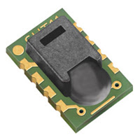
Pressure sensor MPX4100
The pressure sensor (MPX4100) MPX4100 is a pressure sensor that is equipped with signal conditioning circuit and temperature calibrator makes this sensor stable against temperature changes. For this sensor measurement accuracy using micro-machine techniques, thin film metalization and bipolar semiconductor process.

With the signal conditioning circuit, this sensor can connect direct on Analogue to Digital Converter. Signal conditioning circuit generate analog voltage with Full Scale (Full Scale) to 5 Volt. This sensor has the ability to detect the pressure of 15 to 115 kilo Pascal and work under pressure difference between P1 and P2. P1 or Pressure Side consists of gel fluorisilicone that protect it from the objects hard. Pressure sensors on robotic applications are often used as feedback mechanic in which the system microcontroller can detect mechanical condition at the time it. For example to detect strong or weak grip of the robot calculates burden placed on the robot.
Thursday, November 14, 2013
Multiplexer Circuit With Logic Gate
Multiplexer circuit with a logic gate is a multiplexer circuit that utilizes a combination of logic gates.
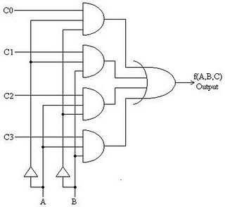
The working principle of the multiplexer circuit above is:
1. Value of bit 00 from the selector will choose the path of the first input as the output
2. Value of bit 01 of the selector will choose the path of the second input as output
3. Value of bit 10 of the selector selects the third input lines as output
4. Value of bit 11 of the selector will choose the four input channels as output
5. As long as there is no change in the bit selector logic condition of the output logic state also will not be amended.
6. If the line selector is connected with a series of counter-up the output to be obtained will represent the input lines in sequence.
7. So it can be concluded that the usefulness of the implementation of a multiplexer function is to satisfy the principle of a simple data distribution. Thus, with multiplexers is possible to transmit data remotely using only one connection.
Read More..
Where the above example can be seen that the circuit has 2 bit selector and 4 input lines. You can make a circuit with more input channels by increasing the number of bits of the selector. And also you can use a combination of gates based on your own design with reference to the previous multiplexer truth table you should specify. So by making a truth table in advance you can easily create a series of logic gates.
The working principle of the multiplexer circuit above is:
1. Value of bit 00 from the selector will choose the path of the first input as the output
2. Value of bit 01 of the selector will choose the path of the second input as output
3. Value of bit 10 of the selector selects the third input lines as output
4. Value of bit 11 of the selector will choose the four input channels as output
5. As long as there is no change in the bit selector logic condition of the output logic state also will not be amended.
6. If the line selector is connected with a series of counter-up the output to be obtained will represent the input lines in sequence.
7. So it can be concluded that the usefulness of the implementation of a multiplexer function is to satisfy the principle of a simple data distribution. Thus, with multiplexers is possible to transmit data remotely using only one connection.
Video Distribution Amplifier
With the amount of equipment during in entertainment centers at present the need to survive able to vary the profit of the audio otherwise capture on film sign is required. I found this instance circuit ready to lend a hand while used in conjunction with the Universal Descrambler and a Stabilizer circuit I built instead of making copies of cassette tapes. It not just allowable me the capacity to fine melody the video strength it and helped me redouble the recorded audio which typically becomes poor as making tape copies. Circuit act is straight redirect designed for amplifier circuits. The minute channel for the audio amplifier is made up of the same components excluding the other partly of IC1 is used. Pin 6 & 5 are inputs and 7 is the output.
 |
| Video Distribution Amplifier |
Temperature and Humidity Sensor
Temperature and humidity sensors used are SHT75. This sensor is a chip that can measure temperature and humidity as well. The use of these sensors with consideration of its small size and reliability. The output of this sensor has the form of digital data in the chip because it has been there for a 14bit ADC.
Temperature measurement range between -40-123,8 º C and humidity between 0-100% Rh. Measurement accuracy reaches ± 0.3 per increase of 25 º C for temperature and ± 1.8% RH for humidity.
Temperature measurement range between -40-123,8 º C and humidity between 0-100% Rh. Measurement accuracy reaches ± 0.3 per increase of 25 º C for temperature and ± 1.8% RH for humidity.
 |
| Temperature and humidity sensor |
The default measurement resolution of this sensor is 14 bits to 12 bits and temperature sensors for humidity sensors, can also use only 12 bit resolution and 8 bits.
Wednesday, November 13, 2013
MPC576H Amplifier Circuit Diagrams
This amplifier circuit has a pretty good quality. Of course the sound quality, although this one amplifier does not have a large output power but in terms of soft and loud voice that this amplifier can be unreliable. With a single IC capitalize MPC576H and several other supporting components you have to make this amplifier circuit. Voltage at least 9 Volt and 24 Volt Max. Output Power 3.5 Watts with 8 Ohm impedance.
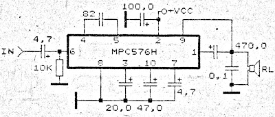
| MPC576H Amplifier Circuit Diagrams |
150W amplifier with active crossover

Series 150W Amplifier With Active Crossover Series 150W Amplifier with Active Crossover is very interesting. Actually, this circuit uses 4-channel power amplifier chip.
Well, as an Active Crossover here we use also a chip that can separate the tone of the bass, midrange and treble, the output from the Active Crossover can be directly amplified by power amplifier.
Well, as an Active Crossover here we use also a chip that can separate the tone of the bass, midrange and treble, the output from the Active Crossover can be directly amplified by power amplifier.
Power Chip 4-channel amplifier that we use is SANYO LA47536 who have power outputs up to 150W, while for Active Crossover (Active Crossover) we use the LF353 from National Semiconductor.

Radio Metal Detector
This metal detector circuit diagram is designed using on a transistor radio as an detector. L1 search coil of the metal detector must have 18 turns from a 0.65 mm enameled wire scrambled on a 4 inch diameter support . The C1 capacitor is a variable capacitor with a value of 365 pF, C2 is a 100pF silver mica capacitor , C3 is a 0.05 uF disc capacitor and the C4 is a 4.7 uF capacitor .
Radio Metal Detector Circuit diagram

The Q1 transistor can be RCA SK3011 npn transistor or equivalent type and all resistors need to be ½ watts . With the radio tuned to a weak station you must adjust the variable capacitor C1 until the locator oscillator beats against the received signal. If a metal is detected the inductance of the L1 coil is changed, changing the frequency of the locator oscillator’s, resulting a change in the beat tone radio .
Radio Metal Detector Circuit diagram
Tuesday, November 12, 2013
Skema Rangkaian Pengapian Motor CDI
The CDI ignition circuit produces a spark from an ignition coil by discharging a capacitor across the primary of the coil. A 2uF capacitor is charged to about 340 volts and the discharge is controlled by an SCR.

A Schmitt trigger oscillator (74C14) and MOSFET (IRF510) are used to drive the low voltage side of a small (120/12 volt) power transformer and a voltage doubler arrangement is used on the high voltage side to increase the capacitor voltage to about 340 volts.
A similar Schmitt trigger oscillator is used to trigger the SCR about 4 times per second. The power supply is gated off during the discharge time so that the SCR will stop conducting and return to its blocking state. The diode connected from the 3904 to pin 9 of the 74C14 causes the power supply oscillator to stop during discharge time. The circuit draws only about 200 milliamps from a 12 volt source and delivers almost twice the normal energy of a conventional ignition circuit.
High voltage from the coil is about 10KV using a 3/8 inch spark gap at normal air temperature and pressure. Spark rate can be increased to possibly 10 Hertz without losing much spark intensity, but is limited by the low frequency power transformer and duty cycle of the oscillator. For faster spark rates, a higher frequency and lower impedance supply would be required. Note that the ignition coil is not grounded and presents a shock hazard on all of its terminals. Use CAUTION when operating the circuit.
An alternate method of connecting the coil is to ground the (-) terminal and relocate the capacitor between the cathode of the rectifier diode and the positive coil terminal. The SCR is then placed between ground and the +340 volt side of the capacitor. This reduces the shock hazard and is the usual configuration in automotive applications.
USB Soundcard Circuit with PCM2702

You do not need to install drivers for Windows XP and Vista, because the driver is already in the system, XP and Vista. So this series is really plug and play.
 |
| Block Diagram |
Description
The core of this construction is a 16-Bit Stereo Digital-To-Analog Converter with PCM2702 USB interface.
 |
| Schematic diagram USB soundcard |
PCM2702 only requires a few additional components to work. This scheme is not complex. The sound card can be activated directly from the USB port (jumper W1) or from an external power supply (jumper W3). PCM2702 requires two 3.3V power supply (3V-3.6V) and 5V (4.5V-5.5V). I use a fixed output voltage to 3.3V LDO TPS76733Q (IO2) and the output voltage is adjusted to 5V LDO TPS76701Q (IO3).
LDO Both are produced by TI, I use it because there in my drawer. Each LDO The same can be used. IO3 output voltage should be set to slightly lower than the input voltage to enable LDO stabilization is good, in my case the output voltage set to 4.8V. output voltage can be set by the resistor R33 is adjusted. In the case of low power supply, IO3 be shorted by the W3 jumper. Signalizes D3 LED power on.
 |
| PCB line design usb soundcard |
 |
| Layout PCB usb soundcard |
Small ferrite beads are placed before all power pins on the PCM2702 and GND Vbus and USB. Small beads reduce high frequency hum. I have a problem finding SMD ferrite beads small local shops but finally I get some of them from the old hard drive. They are not really necessary, you can use zero ohm resistors instead of them.
Low-pass filter placed in the output signal path to reduce the sampling frequency. OPA2353UA dual op amp configured as two stereo-order low-pass filter. Led diodes D1 illuminates when the PCM2702 play audio data received from the USB bus. Diode D2 Led illuminates when the USB bus audio delay the transmission of data to the PCM2702.
 |
| Installed component USB soundcard |
This circuit works very well. I just had shorted crystal during soldering so that circuit does not work, but after removing the short noise, a sound card to work. I have been tested on Windows 2000, XP and Vista. The electronic circuit works in all the systems mentioned. Driver is in the operating system so that the sound card is ready within a few seconds after you connect the electronic circuit is with a PC / Laptop / Notebook you are in trouble with the sound card / sound card that.
During writing this article I have found that the PCM2702 is now not recommended for new designs, but TI offers a better solution. PCM2704, PCM2705 has the same functions as the PCM2702, but they include an output filter. They were able to push the headphones directly.
Volume and mute can be controlled via the SPI bus in PCM2705 or PCM2704 with pushbuttons in the case. PCM2704 and PCM2705 are in TSSOP28 package. PCM2706 PCM2704 and PCM2707 similar to PCM2705 but in addition they have the I2S bus. PCM2706 and PCM2707 are in a TQFP32 package. I recommend using the new chip (PCM2704 / PCM2705) for the new design an Operating System.
10 16 Volt Stereo 2 x 5 5 power amplifier

This amplifier circuit or with it based on ic KA2210 main amplifier, audio amplifier circuit should disupplay minimum of 10 Volt and up to 16 volts. Power output is 2 x 5.5 W stereo amplifier att. By using this amplifier you can listen to the strains of songs from mp3 player, iPod, etc.
This is schematic diagram

Part List
R1 = 4.7R
R2 = 4.7R
C1 = 1uF
C2 = 100uF
C3 = 47uF
C4 = 100uF
C5 = 0.1uF
C6 = 1000uFC7 = 1uF
C8 = 100uF
C9 = 47uF
C10 = 100uF
C11 = 0.1uF
C12 = 1000uFIC = KA2210
Subscribe to:
Posts (Atom)