Monday, September 30, 2013
Touch Sensor Switch Using Inverters
This touch sensor switch can is designed using inverters (N1, N2)and some common electronic components. In standby state at the entrances of N1 there is a signal produced by oscillator N3/N4. At the touch sensor hand capacity forms a bridge to the ground for the 1MHz signal so that the voltage signal at the entrance of N1 decreases more (at the exit of N2 is logical 1). After the release of contact, a signal charge C4 through D1 Mhz, so the output of N2 is 0 logic after short time.
Touch Sensor Switch Using Inverters Circuit Diagram

Installation can be powered with a DC voltage between 3 and 15 volts (maximum current of 2 mA is absorbed).
Touch Sensor Switch Using Inverters Circuit Diagram
AN5265 Amplifier Circuit
Schematic Description :
This Circuit Require voltage 12 -26 Volt. Good Voltage use is 16 Volt , Because its not too small and not too big Voltage. If use voltage that is to large it will quickly damage the IC. And if use voltage that is to small it will make less than maximum sound output.
See this Circuit and datsheet IC AN5265 Below :
 |
| Click to Enlarge |
Datasheet IC AN5265
Vcc = 12-26 V
Pout = 2,3 W
RL = 16 Ohm
Ft = 40hz - 18Khz


Icco = 9,5mA
Package = SIP2-9
Manufactered = MATSUSHITA

LM3886 High Performance Audio Power Amplifier

Audio Power Amplifier is an important part in sound reproduction ina sound system. Audio Power Amplifier with this power IC LM 3886Audio Power Amplifier is a highly capable and able to produce68 Watt power avg. 4Ohm load and capable of producing power 38 Watt8Ohm load.
With good sound reproduction capabilities of 20Hz-20kHz also possessed this LM3886 Audio Power Amplifier. Audio Power Amplifier LM3886 Speaker is equipped with protection that will protect the circuit output from over-voltage, under-voltage, over-loads, a short circuit power supply, thermal run-away and the temperature peak. Audio Power Amplifier LM3886 also equipped with noise reduction that can keep the audio system from noise well.
 |
| Schematic power amplifier with LM3886 |
Feature owned LM3886 Audio Power Amplifier
- 68W cont. avg. output power into 4Ω at VCC = ± 28V
- 38W cont. avg. output power into 8Ω at VCC = ± 28V
- 50W cont. avg. output power into 8Ω at VCC = ± 35V
- 135W instantaneous peak output power capability
- Signal-to-Noise Ratio ≥ 92dB
- An input mute function
- Output protection from a short to ground or to the supplies via internal current limiting circuitry
- Output over-voltage protection against transients from inductive loads
- Supply under-voltage protection, not allowing internal biasing to occur Pls | VEE | + | VCC | ≤ 12V, Thus eliminating turn-on and turn-off transients
- 11-lead TO-220 package
- Wide supply range 20V - 94V
Application of Audio Power Amplifier LM3886
- Stereo audio system
- Active Speaker
- High End Audio Power TV
- Suround Power Amplifier
Sunday, September 29, 2013
LED Driver for Automotive Applications using AT9933
Using the AT9933 variable frequency PWM controller IC, can be designed a very simple and high efficiency LED lamp driver using a low-noise boost-buck topology.The AT9933 uses patent pending hysteretic current-mode control to regulate both the input and the output currents.
This enables superior input surge immunity without the necessity for complex loop compensation. Input current control enables current limiting during startup, input under-voltage and output overload conditions. The AT9933 provides a low-frequency PWM dimming input that can accept an external control signal with a duty cycle of 0 - 100% and a high dimming ratio.

This LED driver electronic project , require an input voltage range between 9 and 16 volts and will provide an 28 volt output at a maximum output current of 350 mA .The switching frequency of this electronic project is 350kHz . Values for components are : L1 = 82μH,L2 = 150μH,C1 = 0.22μF , RCS2 = 1.65Ω 1/4W, RREF2 = 10kΩ 1/8W, RS2A = 100Ω 1/8W,RS2B = 5.23kΩ 1/8W, RCS1 = 0.228Ω 1W, RREF1 = 10kΩ 1/8W,RS1 = 4.42kΩ 1/8W .
This enables superior input surge immunity without the necessity for complex loop compensation. Input current control enables current limiting during startup, input under-voltage and output overload conditions. The AT9933 provides a low-frequency PWM dimming input that can accept an external control signal with a duty cycle of 0 - 100% and a high dimming ratio.
This LED driver electronic project , require an input voltage range between 9 and 16 volts and will provide an 28 volt output at a maximum output current of 350 mA .The switching frequency of this electronic project is 350kHz . Values for components are : L1 = 82μH,L2 = 150μH,C1 = 0.22μF , RCS2 = 1.65Ω 1/4W, RREF2 = 10kΩ 1/8W, RS2A = 100Ω 1/8W,RS2B = 5.23kΩ 1/8W, RCS1 = 0.228Ω 1W, RREF1 = 10kΩ 1/8W,RS1 = 4.42kΩ 1/8W .
Power Supply with principle of UPS

For UPS Power Supply circuit consists of lowering the voltage, rectifier, charger, batery and regulators. The technique is applied from UPS on the power supply is the use of batery and charger is connected dengang direct coupling with a series diode. For more details can be seen with the following image.
 |
| Schematics |
The rectifier in the circuit UPS Power Supply For this to function also as a charger via D1. D3 function is to drain-source voltage of the rectifier to the regulator circuit, when the AC voltage source. D2 serves to drain the batery when the source voltage from AC voltage source does not exist. batery configuration and diode D1, D2 and D3 is adopted from the UPS system. may be useful and can provide inspiration on teman2 all in making backups on the system power supply voltage.
Transformer Electronics

Transformer (transformer) is the electrical / electronics that function to move energy (power) power from input to output or from the primary to the secondary side. The transfer of power from primary to secondary voltage is accompanied by changes either up or down.
There are two types of transformer Raising the voltage transformer (stepup transformers) and lowering the voltage transformer (stepdown transformer).
If the primary voltage is smaller than the secondary voltage, so-called stepup transformer. But if the primary voltage is greater than the secondary voltage, so-called stepdown transformer.At each transformer has primary windings named input and output is called the secondary winding. Has an iron core transformer for low frequency and high frequency ferrite core or some that did not have a core (air core).
When the primary winding given alternating current (AC), the primary windings will be the direction of the magnetic field also magnitnya commute. This magnetic field will induce the secondary winding and secondary winding flows resulted in an alternating current (AC). Suppose the primary coil current flows berfasa positive (+), then the current flowing in the secondary coil berfasa negative (-). Because the current through primary digulungan back and forth, then on the roll sekunderpun flowing alternating current. The amount of charge in the primary winding with the power supplied to the secondary winding. So Pp = Ps or Up.Ip = Us.Is
Where:
Pp = primary power in watts
Ps = power in watts secondary
Up = primary voltage in volts
Us = secondary voltage in volts
Ip = Primary Current in ampere
Is = secondary current in amperes
Example:
A power transformer is connected to the net voltage 220 V, current flowing in primary winding 0.2 amperes. If the secondary voltage of 12 V. Calculate the amount of secondary flow.
Completion:
Up.Ip = Us.Is 220.0,2 = 12. Is Is Is = 44/12 = 3.66 amps
Comparison of transformation:
In general, the number of primary winding is not equal to the number of secondary winding. For stepup transformer primary winding number fewer than the number of secondary winding, contrary to stepdown transformer primary winding amount more than the number of secondary winding. Number of primary winding and secondary winding number shows the amount of voltage primary and secondary tgangan magnitude. The greater the voltage the more the windings. Thus the number of winding is directly proportional to the voltage-enter the respective sides. If the secondary winding and primary winding = Ns = Np, then the ratio of primary winding and secondary winding is called the transformation ratio and expressed as T = Np / Ns. In the transformer equation applies: Up / Us = Np / Ns or T = Up / Us
Example:
A power transformer primary voltage of 220 V, the secondary voltage of 30 V. Number of primary winding 1100 wrap. Calculate the number of secondary winding.
Completion:
Up / Us = Np / Ns = 220/30 = 7.33 1100/Ns 1100/Ns
Ns = 1100 / 7.33 = 150.06 Ns wrap
In the technique known to a variety of electronic transformers, for both high frequency and low frequency. Examples of transformer for high frequency oscillator transformer, transformer intermediate frequency (IF), transformer spull antenna (tuner). While the transformer used for low frequency input transformer, output transformer, transformer filter (choke).
Saturday, September 28, 2013
Circuit Mobile Phone Battery Charger
This post share about Mobile Phone charger circuits, previously you can see other Phone Battery Charger Circuit or Charger Circuit . This Charger ciruit use to charging phone battery using IC 7805 for plus voltage regulator or & 7905 for min voltage regulator. Below is a schematic circuit adapter, power supply, or battery charger (for gadgets, mobile phones, MP4player, smartphone) that is equipped with a 5V voltage stabilizer:
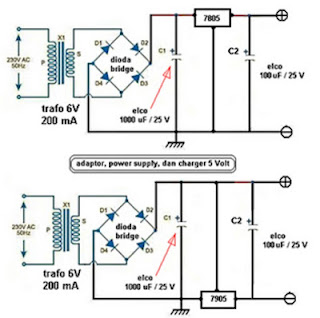
Diode Bridge
diode bridge, known as a diode bridge is used for the rectifier circuit current (rectifier) from AC to DC. to make the diode bridge properly you need to know the type of diode to be used, to suit your needs. example: to make the power supply 12 Volt 3 Ampere diode type 1N5401 is needed, for more detail how to choose the right type of diode to the adapter.
Voltage stabilizers are commonly used are the 78XX or 79XX type LM, XX indicates the maximum voltage output is generated. see the example in the circuit schematic above, to output 5 V is used type LM 7805. for other voltages must be adjusted to the transformer and its stabilizer IC.
Class C Power Amplifier

If the amplifier class B need two transistors to work properly, then there are the so-called class C amplifier that only need 1 transistor. There are few applications that really only requires a positive phase only. An example is the pilot frequency detector and amplifier, RF tuner amplifier circuit and so forth.
Class C transistor amplifier active work only on the positive phase only, even if the need is quite narrow only the peaks are strengthened. Time signal can replica by series resonance of L and C. Typical of the series class C amplifier is like in the following series.
 |
| Basic Schematic Power Amplifier Class C |
The circuit is also not necessary created bias, because the transistor was deliberately made to work the saturation region. Series L C in the circuit will resonate and contributed important in re-replicate input signal into an output signal with the same frequency. This series if given the bait behind can be a series of RF oscillator is often used the transmitter. Class C amplifier have high efficiency even up to 100%, but fidelitas level is more low. But the actual High fidelitas not be purpose of this type of amplifier.
Single Chip 25 Watt Mono Class D Audio Power Amplifier Circuit

This class-D audio ability amplifier is acceptable for TV and home stereo set. TDA7882 IC dent provides class-D audio ability amplifier solution. Since this dent has alone address channel, you charge two pieces of this ambit for stereo application. The ability accumulation voltage is flexible, acquire (+-)10V to (+-)25V. This ambit needs a breach accumulation (symmetric ability supply). Here are the capital appearance of this class-D amplifier:
- 25W OUTPUT POWER: RL = 8 ohm/4 ohm; THD = 10%
- HIGH EFFICIENCY
- WIDE SUPPLY VOLTAGE RANGE (UP TO ±25V)
- SPLIT SUPPLY
- OVER-VOLTAGE PROTECTION
- ST-BY AND MUTE FEATURES
- SHORT CIRCUIT PROTECTION
- THERMAL OVERLOAD PROTECTION
Friday, September 27, 2013
Surround Sound Setup
If you are in the market for a brand new surround sound system Im pretty sure youve been a little baffled by all the options, bells, whistles, gadgets, gizmos, and price tags on the market today. Trust me, you are not alone. One of the most baffling things to many potential surround sound system consumers is where on earth should you put all the speakers. I intend to answer that question and a few more over the course of the next few paragraphs and hope that you will read along.
The first thing you need to understand is that there are several different types of surround sound systems. The industry standard and most common is the 5.1 channel surround sound system. This set up calls for the use of five speakers plus one subwoofer in addition to the receiver. The five speakers are the front speakers which include a left, right, and center speaker and the left and right surround speakers that are located to the left and right from the rear. You should also have a subwoofer located behind you in order to create the bass notes of sound. The next two types of surround sound systems include the 6.1 channel and 7.1 channel system. The primary differences in these are the addition of one additional speaker for each.
You will be glad to know that most receivers will accommodate the 8 total speakers of a 7.1 channel surround sound system but you may want to check in order to be certain you can upgrade if you chose to buy a 5.1 channel system for the time being. The addition of speakers when you upgrade change the layout of the speakers in your home. The more speakers you have, the greater sound you will enjoy, however, the better the quality of your speakers, the better quality your sound will have. In other words dont go with lower quality speakers in the beginning in order to have more speakers, as you will be shooting the quality of sound you can experience in the foot. It is better to buy fewer speakers in the beginning and add to your system over time in order to receive better quality.
When it comes to the placement of the additional speakers if you upgrade to a 6.1 channel surround sound system you will move the speakers currently in the left and right rear to the left and right side and place the new speaker in the center back. If you then upgrade to the 7.1 channel surround sound system you will move the speaker that is in the center to the rear left and place the new speaker to the rear right. This allows you to be literally surrounded by the sound in order to maximize your listening experience.
Of course this is only a recommendation and it is entirely up to you what will work best within your home and according to your tastes and wants in a surround sound system. Not everyone hears music or sound the same and the experience for each will vary greatly from one person to the next. For this reasons it is also a good idea to be sure you have listened to the system in a store before deciding on one and bringing it home. This is a wise decision regardless. I also recommend taking more than one CD or DVD for the listening process in order to make sure the quality is consistent through different mediums.
While the setup of your system is very important to the sound experience it is quite difficult provided you follow the directions (you didnt forget to read those did you?). Whether this is your first home theater or surround sound system or one of many upgrades youve made along the way Im sure you will agree that the sound is far superior to the two speaker systems of days not that long ago.
PPPPP
658
Emergency Lamp using IC 555

Emergency Lamp With 555 is one solution for lighting during power outages. With Emergency Lamp Series 555 uses a 12VDC voltage source that can be supplied from the 12V battery. Emergency Lamp 555 Series With these very simple and easy to make because all the components easily available in the market.
Emergency Lamp Series With this 555 can turn on the light 5W-10W. The circuit is built with an astable multivibrator with the IC 555 that is used to mendrive transformer through Q1. For more details can be viewed directly from the series Emergency Lamp With 555 follows.
 |
| Emergency Lamp Using TLC555 |
Working frequency range of 555 Emergency Lamp With this set of configurations R1, R2 and C2. T1 in series Emergency Lamp With 10V 500mA 555 is a transformer. Secondary part (0-10V) is connected to the Q1 to be given the signal from the multivibrator. Then the primary (0-220V) is connected to the lamp.
Simple Power Amplifier Circuit 2N3055
 |
| Simple Power Amplifier Circuit Diagram |
Transistors:
Tr1 BCY70 (or BC 182L or BC212L or BC214L)
Tr2/3/4 BFY50/51
Tr5 BFX88
Tr6/7 2N3055
Risk of instability if no input connected. When testing, connect R (about 3k3). The Simple Power Amplifier Circuit needs well smoothed power supply of about 20 to 30 volts. Peak power is well over 10 Watts.
Thursday, September 26, 2013
IC LM12 150 Watts high power amplifier
To supply the required voltage to the amplifier circuit minimum of 7 Volt and a maximum of 24 volts . Incurred sizable ouput for amplifier ic 300 W maximum output.

R1_____________________________________10K
R2_____________________________________10K
R3_____________________________________220K
R4_____________________________________2.2R 2W
C1_____________________________________1uF
C2_____________________________________1000uF
C3_____________________________________68pF
D1_____________________________________BY229
D2_____________________________________BY229
L1_____________________________________4MH
IC1____________________________________LM12
Basically the DAC circuit
Basically the DAC circuit is made to meet the need for the level of influence in the development of digital electronic circuits electronics world.
Since the discovery of Silicon and Germanium semiconductor material then quickly there was a revolution in terms of simplicity and accuracy of an electronic circuit. Besides, with the implementation of digital circuits will support at all in terms of data storage and mobility. Lots of data can now be operated with a computer is a data converted from analog signals. For example a voice signal or analog form of video can be played and stored using a computer after analog signals are converted into digital data.
 Advantages possessed by the digital data than analog signal is a certainty the nature of the data or logic. Digital data only can be divided into two kinds of logic high "1" and logic low "0". Logic 1 represents 5 volts and low logic voltage 0 volts represents. Examples of the advantages of digital signals over analog signals is on television or digital radio receiver. By implementing a digital system signals emitted by television or radio stations will form the data 1 and 0, so at the time of the transmission or delivery of data signals that change or damaged by the interruption of transmission will hardly change the logic of the signals. But if the transmitted signal is the original signal in the form of an analog signal then if just a little damage due to interruption of transmission, the signal to be received is a signal that has been damaged serve targeted.
In the DAC circuit above uses two LM741 Op-Amp IC is often used as an amplifier. IC1 to function as a producer of analog signal is reversed, and turned back IC2 function signal from IC1. Basic circuit of the DAC is a common amplifier circuit, only used a variation of several resistors in order to obtain a regular reinforcement signal. Rules that must be understood from this DAC circuit is the value of resistors on the input op-amp. The value for the resistor at high bit (R4) should be 2x the amplifier resistor (R5), then for the next bit should be 2x the resistor value at a higher bit. So if the circuit uses 4-bit DAC is the unit bit (lowest bit) is the value of bits to be 8x-4. From the picture above the unit bit is represented by resistor 80 Kohm.
Sample Conditions:
- 0001 (1) = switch SW1 closed and others opened, the voltage output produced is (5K/80K) x 9 volt = 0.5625 volts
- 0010 (2) = SW2 is closed and another switch is opened, the output voltage is (5K/40K) x 9 volts = 1.125 volts
- 0011 (3) = SW1 and SW2 is closed and another switch is opened, the voltage output is (5K/Rparalel 80K and 40K) x 9 volt = (5K/26, 667K) X 9 volt = 1.6875 volts
- 1000 (8) = SW4 is closed and another switch is opened, the output voltage is (5K/10K) x 9 volts = 4.5 volts.
From the above calculation can be concluded that unlicensed with a voltage output proportional to the input conditions, eg for 1 decimal is 0.5625 volts then, decimal 2 = 2 x 0.5625 = 1125 volts, decimal 3 = 3 x 0.5625 = 1.6875 volts, and so on. This condition is due to the parallel relationship between the input resistors.
Read More..
Since the discovery of Silicon and Germanium semiconductor material then quickly there was a revolution in terms of simplicity and accuracy of an electronic circuit. Besides, with the implementation of digital circuits will support at all in terms of data storage and mobility. Lots of data can now be operated with a computer is a data converted from analog signals. For example a voice signal or analog form of video can be played and stored using a computer after analog signals are converted into digital data.
In the DAC circuit above uses two LM741 Op-Amp IC is often used as an amplifier. IC1 to function as a producer of analog signal is reversed, and turned back IC2 function signal from IC1. Basic circuit of the DAC is a common amplifier circuit, only used a variation of several resistors in order to obtain a regular reinforcement signal. Rules that must be understood from this DAC circuit is the value of resistors on the input op-amp. The value for the resistor at high bit (R4) should be 2x the amplifier resistor (R5), then for the next bit should be 2x the resistor value at a higher bit. So if the circuit uses 4-bit DAC is the unit bit (lowest bit) is the value of bits to be 8x-4. From the picture above the unit bit is represented by resistor 80 Kohm.
Sample Conditions:
- 0001 (1) = switch SW1 closed and others opened, the voltage output produced is (5K/80K) x 9 volt = 0.5625 volts
- 0010 (2) = SW2 is closed and another switch is opened, the output voltage is (5K/40K) x 9 volts = 1.125 volts
- 0011 (3) = SW1 and SW2 is closed and another switch is opened, the voltage output is (5K/Rparalel 80K and 40K) x 9 volt = (5K/26, 667K) X 9 volt = 1.6875 volts
- 1000 (8) = SW4 is closed and another switch is opened, the output voltage is (5K/10K) x 9 volts = 4.5 volts.
From the above calculation can be concluded that unlicensed with a voltage output proportional to the input conditions, eg for 1 decimal is 0.5625 volts then, decimal 2 = 2 x 0.5625 = 1125 volts, decimal 3 = 3 x 0.5625 = 1.6875 volts, and so on. This condition is due to the parallel relationship between the input resistors.
Low Voltage Amplifier Circuit with IC BA518
This Circuit use IC BA518 or you can use the IC BA547 , this is low mono power amplifier. Maximum power output 5W . But this is also low voltage amplifier with minimum voltage require 2 Volt. And maximum voltage 12 Volt .Impedance 8 Ohm , support small speakers.Circuit schematic below :
 | |
| Click image to view large |
Troubleshooting if circuit not working :
- Check components are can be use or not , also check the use avometer or other measuring instrument.
- Check the voltage on each component.
- If there is a voltage that has not been entered on the components, then see if there is a broken line or short-circuit PCB , thereb inhibiting the incoming flow.
- Then check whether the input and output cables are still good or not.
Wednesday, September 25, 2013
High Voltage White LED Driver
This high voltage white LED driver electronic circuit schematic is based on the NCP5021 IC manufactured by On Semiconductor . This NCP5021 high voltage white LED driver electronic circuit is designed with ambient light sensing feature . The NCP5021 white LED driver is capable of driving up to 8 LEDs in series for portable backlight applications. The built−in DC DC converter is based on a high efficient PWM boost structure with 32 V output voltage span. The schematic circuit is very simple , requiring few external electronic parts and it can be connected through an I2C protocol to another device or microcontroller .
High Voltage White LED Driver Circuit diagram

Main features of the NCP5021 high voltage LED driver are : 2.7 to 5.5 V Input Voltage Range , 90% Peak efficiency with 4.7 _H / 150 m_ Inductor , Gradual Dimming Built−in (Automatic Fade In/Fade Out Effect) , Integrated Ambient Light Sensing Automatically Adjusts the LCD , Backlight Contrast , Support the Full I2C Protocol with Address Extension . NCP5021 is a high voltage LED driver is specially designed for backlight driver in applications like : Cellular Phone, Smartphone , Portable Media Player (PMP) , Global Positioning System (GPS) .
The circuit application for the NCP5021 require just few external components as you can see in the circuit application from the schematic.
High Voltage White LED Driver Circuit diagram
Main features of the NCP5021 high voltage LED driver are : 2.7 to 5.5 V Input Voltage Range , 90% Peak efficiency with 4.7 _H / 150 m_ Inductor , Gradual Dimming Built−in (Automatic Fade In/Fade Out Effect) , Integrated Ambient Light Sensing Automatically Adjusts the LCD , Backlight Contrast , Support the Full I2C Protocol with Address Extension . NCP5021 is a high voltage LED driver is specially designed for backlight driver in applications like : Cellular Phone, Smartphone , Portable Media Player (PMP) , Global Positioning System (GPS) .
The circuit application for the NCP5021 require just few external components as you can see in the circuit application from the schematic.
Capacitor leakage circuit tester
Generally capacitor that complement with television circuit is often leaked. Consequently spots more rugged display disturbing images running. This is not desired by the owner is not it? For those who know about electronics is certainly a problem. They will find the cause and trying to fix it. For it is not uncommon to use multitester a a search tool damage. But for those who do not have a tool that becomes an obstacle . However , for those of you who enetered last category do not sad because they can assemble their own tester. This tool is very simple but very sensitive to the leackage of a capacitor.
 |
| Schematic |
Resistor
R1____________________________3K3
R2____________________________100K
R3____________________________100K
Capacitor
C1____________________________10uF 150V
C2____________________________10uF 150V
Diode
D1____________________________K-200
D2____________________________K-200
Lamp__________________________Fluorescent Lamp
Switch_________________________On/Off
How to test the capacitor which is in the television circuit or the other device are a follows :
- The early circuit of television or other is turned on. Then look at the picture on the screen (for television) . If the images on television rough then opened the real pole. Then the jack that connects the fluorescent lamp is connected to negative leg. If the light is on or blinking so the capacitor is in good condition. But that does not turn mean capacitor is damaged.
- Next soldering in place. Remove capacitor legged leg positive. Connect the cable from the switch . The the switch is pressed. Contacs occur between the components with each other previously linked. When the fluorescent lamp is lit, we can be sure the capacitor is still good. And if otherwise , capcitor is damaged.
Mono Power Amplifier A1015 BD140 TIP2955
Typically audio amplifier stereo amplifier to a two amplifier. And if a mono amplifier is a single speaker. However this circuit command be present extended to the mono two loudspeaker.But not a equivalence or else serialization access.This makes it needless impedance of the speaker has altered.But will remain to utilize the spokeswoman as a replacement for of the resistance - Collection Peter (RC) of the transistor.The circuit can be alive prolonged to 2 loudspeaker itself.
 |
| Mono Power Amplifier - A1015, BD140 ,TIP2955 Circuit Diagram |
What time raising the power supply circuit and the audio to input. the audio sign coupling to through the C1 and R1 to increase with the Q1.Which Q1 serves like the Regional Pre amp amplifier to power up to a one point.already conveyance it to Q2.Which Q2 is connected to emitter follower circuit.be active as a driver amplifier intimate section from the pre amp section provides added power to drive the Q3 perform. and Q3 motivation provide while a Regional Power amp amplifier output to the spokeswoman.The opinion of the audio intimate through the VR1 and R2 to enter the pin B of Q2.To control the stability of working instead of well brought-up.This circuit is an output of 40 milliwatts watts of distortion of the gesture rate is by the side of 0.1 percent.And frequency response from 15 Hz - 200 kHz.
Tuesday, September 24, 2013
50 ohm dummy load
Assemble their own 50 ohm dummy load with a capacity of 40 watts. first of all we need is a 1k resistor 2watt as many as 20 seeds, plain PCB, and also the female connector just as the picture above. The first step is the form of a round PCB with the above picture just as much as 2 pieces of 3 cm diameter, to which drilled the diameter of the connector.

With the goal as a PCB connector while the other will not need to be drilled due to the bottom. two pairs of resistors that is just as in the picture. if the test is finished living, 50 g 0hm what? if the resistor is not needed to be corrected again. What if want a bigger watt capacity, we simply replace the resistor, 1K5 ato 2k, of course, if using a 2k resistor smakin much we need. resistor which point no matter how much we want to attach. critical values should be 50 ohms and the value of each resistor must be equal. survived the experiment may be useful
2 4GHz WiFi ISM Band Scanner Description and Schematic Part 1
Have you ever wondered exactly what is going on in the 2.4GHz WiFi and ISM band around your house. What channel is it best to set your wireless router to? Why are you getting such poor performance across your WiFi network? Is your neighbour on the same frequency?
Just what is out there? This neat little gadget will sniff the airwaves and give you a graph of the signal strength vs frequency across the entire band. It connects to your computer by USB 2.0 and with the companion Windows software you can display the spectrum or save the raw data to an Excel compatible file for some more number crunching.

It uses just two significant components, a radio module from Cypress Semiconductor and a PIC microcontroller from Microchip. Total cost to build it should be less than US$30.
The 2.4GHz Band
The 2.4GHz ISM (Industrial Scientific Medical) band is often called the WiFi band because it is used for WiFi networking (ie, 802.11 b/g/n). This band is unlicensed, meaning that you and anyone can transmit on it. As a result it has been used by a multitude of products including video transmitters, portable telephones, Bluetooth devices, wireless keyboards, toys and so on. Because you cannot see what is going in the band on you can experience strange behaviour from your wireless gadget. All of a sudden your wireless keyboard skips characters, is it because someone is using a portable phone on the same frequency?
The biggest victim is WiFi networking. This needs a lot of bandwidth, is always transmitting and is sensitive to interference. This is why people often cannot get a decent range from their wireless network and give up in disgust.
This scanner will draw a graph on your computer screen showing you the activity across the band and indicate the best frequencies to use. If you use a laptop you can also wander around and identify the culprits that are clogging the airwaves.
How It Works
Internally the scanner is very simple. It just contains a radio receiver and a microcontroller…

The radio receiver is the Cypress CYWUSB6935 Radio SoC (System on a Chip). This is a complete low power radio transmitter/receiver chip for the 2.4GHz band and is controlled by a microcontroller over a synchronous serial (SPI) interface. The microcontroller can write to various registers in the chip to set things like operating frequency and can read other registers to retrieve data from the chip.
This chip is designed to operate over the 2.4GHz band and has the ability to listen on a frequency for any other devices that may be already using the frequency. This is to help the microcontroller select a suitably free frequency before transmitting. The chip reports the signal level as a number typically up to 30, with zero representing no signal. We use this facility in this project - simply put, the microcontroller instructs the module to step to a frequency and measure the signal level at that frequency, when done it steps the chip to the next frequency and instructs it to measure the signal level there. And so on, right across the band.
We actually do not use the transmit/receive function, which is normally the chips main purpose in life.
The microcontroller used in this project is the Microchip PIC18F2550 which integrates the complete USB 2.0 functionality. The microcontroller sets the radio chip to a frequency, reads the signal level from the chip, stores the value in its internal memory and steps on to the next frequency. This continues until the complete 2.4GHz band is covered. The 18F2550 then sends the data off to your computer using USB and your computer, using custom software, displays the resultant spectrum.
Physically the scanner is just a small box hanging on the end of a USB cable.
The Circuit
The circuit is the simplest part of this project. Click on the image or go to the download section at the bottom of this page for a full scale drawing.
Just what is out there? This neat little gadget will sniff the airwaves and give you a graph of the signal strength vs frequency across the entire band. It connects to your computer by USB 2.0 and with the companion Windows software you can display the spectrum or save the raw data to an Excel compatible file for some more number crunching.
It uses just two significant components, a radio module from Cypress Semiconductor and a PIC microcontroller from Microchip. Total cost to build it should be less than US$30.
The 2.4GHz Band
The 2.4GHz ISM (Industrial Scientific Medical) band is often called the WiFi band because it is used for WiFi networking (ie, 802.11 b/g/n). This band is unlicensed, meaning that you and anyone can transmit on it. As a result it has been used by a multitude of products including video transmitters, portable telephones, Bluetooth devices, wireless keyboards, toys and so on. Because you cannot see what is going in the band on you can experience strange behaviour from your wireless gadget. All of a sudden your wireless keyboard skips characters, is it because someone is using a portable phone on the same frequency?
The biggest victim is WiFi networking. This needs a lot of bandwidth, is always transmitting and is sensitive to interference. This is why people often cannot get a decent range from their wireless network and give up in disgust.
This scanner will draw a graph on your computer screen showing you the activity across the band and indicate the best frequencies to use. If you use a laptop you can also wander around and identify the culprits that are clogging the airwaves.
How It Works
Internally the scanner is very simple. It just contains a radio receiver and a microcontroller…
The radio receiver is the Cypress CYWUSB6935 Radio SoC (System on a Chip). This is a complete low power radio transmitter/receiver chip for the 2.4GHz band and is controlled by a microcontroller over a synchronous serial (SPI) interface. The microcontroller can write to various registers in the chip to set things like operating frequency and can read other registers to retrieve data from the chip.
This chip is designed to operate over the 2.4GHz band and has the ability to listen on a frequency for any other devices that may be already using the frequency. This is to help the microcontroller select a suitably free frequency before transmitting. The chip reports the signal level as a number typically up to 30, with zero representing no signal. We use this facility in this project - simply put, the microcontroller instructs the module to step to a frequency and measure the signal level at that frequency, when done it steps the chip to the next frequency and instructs it to measure the signal level there. And so on, right across the band.
We actually do not use the transmit/receive function, which is normally the chips main purpose in life.
The microcontroller used in this project is the Microchip PIC18F2550 which integrates the complete USB 2.0 functionality. The microcontroller sets the radio chip to a frequency, reads the signal level from the chip, stores the value in its internal memory and steps on to the next frequency. This continues until the complete 2.4GHz band is covered. The 18F2550 then sends the data off to your computer using USB and your computer, using custom software, displays the resultant spectrum.
Physically the scanner is just a small box hanging on the end of a USB cable.
The Circuit
The circuit is the simplest part of this project. Click on the image or go to the download section at the bottom of this page for a full scale drawing.
2.4GHz WiFi & ISM Band Scanner Circuit Diagram

The PIC 18F2550 microcontroller is a 28 pin part with a built in USB 2.0 interface. As mentioned before, the chip integrates everything connected with the USB including a 3.3V regulator, memory buffers and the USB transceiver. All that you need to do is to connect the USB cable to pins 15 and 16 of the chip and place a capacitor on pin 14 to help smooth the inbuilt 3.3V supply.
The clock for the microcontroller is derived from the 20MHz crystal with the two 15pF capacitors providing the correct loading for the crystal. Internally within the 18F2550 the 20MHz is divided by 5 to give 4MHz and then used to synchronise a phase locked loop (PLL) oscillator running at 48MHz. This is the main clock used within the microcontroller and is used to drive both the USB interface and the CPU. Running at 48MHz this is a speedy little chip so we do not have any issues with performance.
The ISCP connector is there so that I could reprogram the 18F2550 without pulling it out of its socket. It is mostly used for prototyping so you can leave it out if you want. Note that the 10K resistor on pin 1 of the 18F2550 is still needed to pull the reset line high.
Power for the circuit is drawn from the +5V supplied by the host computer on the USB cable. The whole circuit only draws a few tens of milliamps so it is not a significant load. This 5V is dropped to about 3V by three 1N4001 diodes to provide power for the Cypress CYWUSB6935 chip which is mounted on a small PCB (the CYWM6935 module). Each diode will drop about 0.7V resulting in a total voltage drop of about 2V. This is a crude way to derive a 3V supply but it is low cost and does the job without any hassles.
The CYWUSB6935 chip has protective diodes on its inputs, which clamp the signal line to its power supply (3V). This means that we can drive it with 5V signals from the microcontroller with series resistors to limit the current. This is the purpose of the 3.3K resistors, they limit the current in the clamping diodes to less than a milliamp when the PICs output goes to 5V.
CYWM6935 Module
The CYWUSB6935 chip comes in a tiny package designed for machine assembly and is virtually impossible for a mortal wielding a soldering iron to solder. Fortunately Cypress have assembled it into the CYWM6935 module along with two aerials, a crystal and a few capacitors. The connector used in the module is still rather tiny and non standard (or rather it does not use the 0.1" grid that we know and love), but it can be soldered to. For details of the CYMUSB6935 chip and CYWM6935 module go to here.

Parts Listing
- 1 x Microchip PIC18F2550-I/SP microcontroller programmed with the firmware available in the download section at the bottom of this page.
- 1 x Cypress CYWM6935 radio module,
- 1 x 20MHz crystal
- 3 x 1N4001 silicon diodes
- 4 x 3.3K resistors (quarter or half watt)
- 1 x 10K resistor (quarter or half watt)
- 2 x 15pF ceramic capacitors
- 1 x 100nF multilayer ceramic capacitor 1 x 220nF polyester capacitor
- 1 x 100uF electrolytic capacitor (6V or higher)
- 1 x 28 pin IC socket
- 1 x USB cable with a type A connector on one end
- 1 x UB5 jiffy box
IR Remote Control Extender Mark 3
This Mark3 version of the Infra Red extender is a special version designed to control appliances that use high frequency modulated IR remote controls.

Notes:
IR appliances use pulses (control signals) sent over a modulated IR carrier wave. The carrier wave may be modulated at various frequencies, 36-38KHz being the most popular.Some Satellite receivers use even higher frequencies than this. The IR1 remote module receives an infra red signal and separates control pulses from the modulation. To re-transmit, a 555 timer is configured as an astable oscillator. The 555 timer is controlled by the signal on the reset pin, high generating a carrier and low no carrier. Each control pulse turns on the oscillator for the duration of a logic high signal and off for a logic 0 signal, thereby creating a newly modulated IR signal. The IR module, part number IR1 is available from Harrison Electronics in the UK, IR1 may not be listed in their catalogue but if you ask for an IR1, they will send you the correct part. The IR1 arrives in a small aluminium case, the connections viewed from underneath are shown below:
Infra Red Module, IR1 Pinout

Harrison Electronics have limited supplies of the IR1 but as a replcement a standard IR module like the TSOP1838 may be used. The pinout is shown below:

The carrier frequency is determined by R1 and C3, values shown work at 39.7 kHz, but these may be altered to provide different carrier frequencies. The final CMOS 4049 invertor ensures that under "no signal" conditions both LEDs are also off.
Parts List:
C1 100u 10V
C2 100n polyester
C3 120p silver mica
C4 100n polyester
R1 150k
R2 2k2k
R3 1k
R4 47R 1W
Q1 BC109C
IC1 LM7805
IC2 555
IC3 IR1 module from Harrison Electronics or TSOP1838
IC4 4049 CMOS Invertor LED1 Red LED (or any visible colour)
LED2 TIL38 or part YH70M from Maplin Electronics
PCB Layout (courtesy of Claudio from Italy):
First the component side of the board is shown below.
.png)
And now thw pcb itself.

The Mark 3 circuit is an improvement over the Mark 1 and 2 circuits, however the drive from Q1 inverts the polarity of the output pulse. In some cases this can cause problems so the output stage is rewired as an emitter follower. This is the basis for the Mark 4 circuit. If you still have problems then I would recommend trying the Mark 4 circuit.
IR appliances use pulses (control signals) sent over a modulated IR carrier wave. The carrier wave may be modulated at various frequencies, 36-38KHz being the most popular.Some Satellite receivers use even higher frequencies than this. The IR1 remote module receives an infra red signal and separates control pulses from the modulation. To re-transmit, a 555 timer is configured as an astable oscillator. The 555 timer is controlled by the signal on the reset pin, high generating a carrier and low no carrier. Each control pulse turns on the oscillator for the duration of a logic high signal and off for a logic 0 signal, thereby creating a newly modulated IR signal. The IR module, part number IR1 is available from Harrison Electronics in the UK, IR1 may not be listed in their catalogue but if you ask for an IR1, they will send you the correct part. The IR1 arrives in a small aluminium case, the connections viewed from underneath are shown below:
Infra Red Module, IR1 Pinout
Parts List:
C1 100u 10V
C2 100n polyester
C3 120p silver mica
C4 100n polyester
R1 150k
R2 2k2k
R3 1k
R4 47R 1W
Q1 BC109C
IC1 LM7805
IC2 555
IC3 IR1 module from Harrison Electronics or TSOP1838
IC4 4049 CMOS Invertor LED1 Red LED (or any visible colour)
LED2 TIL38 or part YH70M from Maplin Electronics
PCB Layout (courtesy of Claudio from Italy):
First the component side of the board is shown below.
Low power amplifier with IC TA7140
Low power amplifier with based on the IC (intregated circuit) TA7140 manufactered by TOSHIBA , its have original output power is 0,15 Watts, and the schematic diagram is monolithic power amplifier.Though the amplifier circuit has a low output , but the maximum voltage large enough to 30 volts.

Part List :
Resistor = 100R
Capacitors = 4u7F , 33uF , 100uF , 1000nF , 4700nF , 47uF
IC = TA7140P
Technical information :
Max. Voltage = 30 V
Min. Voltage = 5 V
Max. Output = 1 W
RL = 150 Ohm
Monday, September 23, 2013
Headset amplifier via USB
Headset amplifier via USB circuit is a series that is used to add a gain on the headset, which is used on a computer headset. Indeed not only on a computer course in all the headset could also, but in the above circuit voltage to utilize voltage mensupply issued on a PC or laptop via USB. So you need not bother looking for supply voltage, you just take it from USB.
 Part List :
Resistor
R1 = 20K
R2 = 10K
R3 = 10K
Capacitor
C1 = 3u3F 50V
C2 = 100pF
Diode
D1 = 1N4148
D2 = 1N4148
D3 = 1N4148
D4 = 1N4148
IC
U1 = JRC4558
Connector X1
1 = Output
2 = Input
3 = Ground
Connector X2
1 = V+ 5V from USB
2 = Ground From USB
Resistor
R1 = 20K
R2 = 10K
R3 = 10K
Capacitor
C1 = 3u3F 50V
C2 = 100pF
Diode
D1 = 1N4148
D2 = 1N4148
D3 = 1N4148
D4 = 1N4148
IC
U1 = JRC4558
Connector X1
1 = Output
2 = Input
3 = Ground
Connector X2
1 = V+ 5V from USB
2 = Ground From USB
 |
| PCB design Views |
2 3 Watt Low audio power amplifier

These amplifiers using IC KA2202 and KA2207, which has a power output of 2.3 Watt berimpedansi 4 ohms. Minimum supply voltage and maximum 5Volt 20Volt. See schematics and component list below.
Part List
R1 = 100K
R2 = 56R
R3 = 56R
R4 = 1R
Use 1/4 Watt resistor

C1 = 100uF
C2 = 100uFC4 = 100uF
C5 = 470uFC6 = 100nF
C7 = 470pFC8 = 2,2nF
C9 = 100uF
U1 = KA2202 , KA2207
2 Transistor Line Follower Robot
Make a line follower robot can be done with two transistors. Line Follower Robot series is one of the two transistors contor robot line follower circuit is in Bagun with two NPN transistor and the motor driver as well as processing of sensor signals.
In the circuit of line follower robot consists of two parts of the same, only different functions for the motor driver the right and left. Sensor circuit of line follower robot uses the LDR and LED. LDR sensor sensitivity can be set with the VR 10 is mounted in series with the LDR. For more details, see the following figure.
In the circuit of line follower robot consists of two parts of the same, only different functions for the motor driver the right and left. Sensor circuit of line follower robot uses the LDR and LED. LDR sensor sensitivity can be set with the VR 10 is mounted in series with the LDR. For more details, see the following figure.
Line Follower Robot series 2 Transistor
The working principle of the motor driver circuit between the right and left together, when the LDR get the reflection of light from the LED LDR resistance will decrease and make the transistor saturation and motor gets supply and rotates so that the robot moves forward. So at the moment is not the case then the motor did not get a supply, for example, only one sensor is exposed line and make the LDR did not receive the reflected light is then Motr in the stationary and the other motor rotates and makes the LDR are back in the reflection of light and the robot moves forward again.
Line Follower Robot
Sunday, September 22, 2013
2 4GHz WiFi ISM Band Scanner Assembly Using the Scanner Part 3
2.4GHz WiFi & ISM Band Scanner. Description and Schematic - Part 1
2.4GHz WiFi & ISM Band Scanner. Firmware and Sowtware - Part 2
Assembly
Because the circuit was so simple I took the easy way out and assembled it on a piece of veroboard. Nowadays I would design my own printed circuit board (see custom PCBs).
Rather than finding a connector for the Cypress module I simply soldered single core hookup wire directly to the connector pins. This supported the module and allowed me to position it away from the microcontroller to minimise interference.
The USB cable was made from a standard USB cable with type A and B connectors, I just cut off the B connector and soldered the wires directly to the veroboard with half an inch of heatshrink tubing to keep it neat. That left the type A connector at the other end, ready to plug into the computer.
Note that the red and black wires in the USB cable are +5V and ground respectively. You should check these with a multimeter before soldering them in. The green wire is normally D+ and goes to pin 16 of the 18F2550 while the white is D- and goes to pin 15. The shield does not have to be connected.
The final touch was to drop the assembly into a standard UB5 "jiffy" box with a notch cut out for the USB cable to pass through.

Using the Scanner
With nothing running in the immediate vicinity you will just see background noise, as shown in the screen shot below.

Note that the vertical scale is not calibrated to any particular scale. In fact the scale is just the signal level "factor" reported by the Cypress radio module.
The base level signal represents the noise in the air and in the radio receiver part of the module.
The screenshot below shows a WiFi 802.11n wireless router running on channel 1 and located about 12 metres from the scanner. As you can see the 802.11n (and for that matter 802.11g) routers spread themselves over six channels.

That is the good thing about using channel 1 and 13 for your WiFi setup, you get some unused channels on one side where your spectrum can spread into.
But, using channel 13 has its own problems.
The spectrum on the next screenshot is identical to the one above but this time my microwave oven was heating up dinner. Incidentally, the microwave oven was nothing special, just a domestic model and about 10 metres from the scanner.

As you can see, it totally blotted out the higher frequency end of the band. All microwave ovens seem to use this part of the band and you cannot blame the microwave for their activity, as this was part of the reason for setting up the 2.4GHz ISM band in the first place. Avoiding the microwave oven interference and having some free spectrum on one side is the reason why channel 1 is the best choice for your router (assuming your neighbour has not got there first).
Finally, the screenshot shows a Bluetooth mouse communicating with a computer.

Bluetooth hops all over the 2.4GHz band as it finds the best spots with the minimum of interference. Spikes all over the spectrum is a good indicator of Bluetooth activity.
2.4GHz WiFi & ISM Band Scanner. Firmware and Sowtware - Part 2
Assembly
Because the circuit was so simple I took the easy way out and assembled it on a piece of veroboard. Nowadays I would design my own printed circuit board (see custom PCBs).
Rather than finding a connector for the Cypress module I simply soldered single core hookup wire directly to the connector pins. This supported the module and allowed me to position it away from the microcontroller to minimise interference.
The USB cable was made from a standard USB cable with type A and B connectors, I just cut off the B connector and soldered the wires directly to the veroboard with half an inch of heatshrink tubing to keep it neat. That left the type A connector at the other end, ready to plug into the computer.
Note that the red and black wires in the USB cable are +5V and ground respectively. You should check these with a multimeter before soldering them in. The green wire is normally D+ and goes to pin 16 of the 18F2550 while the white is D- and goes to pin 15. The shield does not have to be connected.
The final touch was to drop the assembly into a standard UB5 "jiffy" box with a notch cut out for the USB cable to pass through.
Using the Scanner
With nothing running in the immediate vicinity you will just see background noise, as shown in the screen shot below.
Note that the vertical scale is not calibrated to any particular scale. In fact the scale is just the signal level "factor" reported by the Cypress radio module.
The base level signal represents the noise in the air and in the radio receiver part of the module.
The screenshot below shows a WiFi 802.11n wireless router running on channel 1 and located about 12 metres from the scanner. As you can see the 802.11n (and for that matter 802.11g) routers spread themselves over six channels.
That is the good thing about using channel 1 and 13 for your WiFi setup, you get some unused channels on one side where your spectrum can spread into.
But, using channel 13 has its own problems.
The spectrum on the next screenshot is identical to the one above but this time my microwave oven was heating up dinner. Incidentally, the microwave oven was nothing special, just a domestic model and about 10 metres from the scanner.
As you can see, it totally blotted out the higher frequency end of the band. All microwave ovens seem to use this part of the band and you cannot blame the microwave for their activity, as this was part of the reason for setting up the 2.4GHz ISM band in the first place. Avoiding the microwave oven interference and having some free spectrum on one side is the reason why channel 1 is the best choice for your router (assuming your neighbour has not got there first).
Finally, the screenshot shows a Bluetooth mouse communicating with a computer.
Bluetooth hops all over the 2.4GHz band as it finds the best spots with the minimum of interference. Spikes all over the spectrum is a good indicator of Bluetooth activity.
Dayton Audio 150W Power Amplifier
Dayton Audios versitile APA150 can liberate 75 watts into 2 channels, or else 150 watts into 8 ohms what time hard to suspension bridge-mono mode. A built-all the rage, switchable low-pass filter makes this a huge subwoofer amp, and bursting range line-level outputs allow in lieu of bi-amp configurations.

Technical Details :
close to racket-uninhibited fan company in support of reach deal with applications
lustrous prevailing design looks safe participating in a few audio structure
shrill current, discrete output transistors so as to run cool and subdued
flexible 50-150 Hz low pass crossover gives you the span control you need
Dayton Audio APA150 150W Power Amplifier
Stereo Balance Indicator

Mechanical deficiencies that affect the reproduction of sound in a stereo amplifier is probably what you are thinking, armpit all the problems have been overcome. And actually bigger role than we know. True, the effect is so small that only a few of us who record it, or divert it to other things.
Most of such shortcomings can be traced back toto the stereo volume control ,maybe two in the no -stepresistance . As a result, the volume difference arises between the two channels and can usually be in balance again by the regulator balance. If you intend to define these differences precisely, stereo balance these indicators can fulfill your purpose.
 |
| Stereo Balance Indicator circuit |
Quite simply, this circuit by connecting the output terminal and the right channel loudspeaker left channel of the amplifier and feed the same signal, should sinusoid (or cues mono) to the second input channel amplifier. If then the signals at both terminals tarafnya exact same loudspeakers, meters (zero in the middle) in the indicator of this balance will not deviate. However, if the signal level in the left channel is higher than the right channel meter will deviate to the left (or right if the opposite occurs). In this regulatory balance can be set up to read something about zero feet again, then the effect of volume control tracking error can be eliminated.
Trimpot P1 on balance the indicator should be set for full scale meter deflection, when only one channel worked.
Saturday, September 21, 2013
Audio amplifier with IC AN7522 AN7523 and TDA2616

The series of amplifiers that are used on the television audio, amplifier used amplifier ICs, including the IC:
• AN7523• AN7522
• TDA2616
Third series of the function with the same system, namely BTL (Bridge Transformer Less). By using such configuration we get several advantages, namely no use coupling capacitors or coupling transformers.
Block diagram of circuit in the IC AN7522, AN7523 and TDA2616 as in the image below :
 |
| Schematic AN7522 |
 |
| AN7523 amplifier schematic |
 |
| Schematic TDA2616 |
Subscribe to:
Posts (Atom)