Showing posts with label circuit. Show all posts
Showing posts with label circuit. Show all posts
Friday, November 22, 2013
Amplifier Circuit with IC AN7143
On this Integrated circuit power amplifier use IC AN7143 but you can use this following IC :
| AN7147 | HA1377 |
| AN7149N | HA1377A |
| AN7168 | HA1392 |
| AN7169 | HA1398 |
| AN7176 | HA13102 |
| AN7178 | HA13108 |
| M5160L | ULX3777 |
You can use all the IC above on this circuit below :

This Circuit require minimum voltage 9 volt , and Maximum voltage 24 volt. Supply voltage with dual voltage not triple voltage. Maximum Output power 2 X 20 watt , with minimum impedance 4 Ohm. This is a stereo power amplifier Circuit. Notif the similiar IC have each distinct power.

Thursday, November 21, 2013
450W audio power amplifier circuit
 Below it is a circuit of power amplifiers with power output of 450 watts mono , amplifiers are also frequently used in the amplifier a high-power amplifier, which used in an event, in the field and the placed closed. Because this amplifier suitable for the woofer, fullrange speaker, and can also be fixed for the subwoofer speaker.
To further strengthen and maximize the amplifier ,its power supply circuit also must be accurate, for electrolytic capacitors in power supply ,voltage capacitors use 80V or more, and a capcity 20000uF upwards, so when the bass amplifier is high , the voltage is not lot of experience dropping. Diode bridge use a minimum of 35A, or adjust the current input voltage. If the power supply has fulfilled the desire, the supply to the power amplifier.

Tuesday, November 19, 2013
6 Watt 4 Ohm Amplifier Circuit
This is an audio amplifier circuit based on IC, and IC were used that MPC563 with minimal output 6W, with impedance of 4 Ohm. Supply Voltage Minimum 4 Volt DC and a maximum voltage to 20 Volts DC. See him under this Scheme.
 |
| 6 Watt 4 Ohm Amplifier Circuit |
Sunday, November 17, 2013
Series electric circuit
Series electrical circuit is an electrical circuit, in which the input of a component derived from the output of other components. This has led to a series electrical circuit can save costs (fewer connecting cables used). In addition to own excess, a series electrical circuit also has a weakness, if one component is removed or damaged, then the other components will not function properly. Eg light bulbs strung together three series, the input of a single lamp light output will come from the other. If one lamp removed or damaged, then the other lights will go off. Consider the following series of three lights :
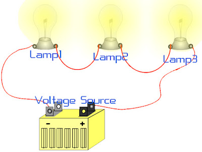 |
| Series electric circuit of three lights. |
Replacement series resistance equation can be sought from the initial equation, in which a strong electric current on each of each hambaran is the same, while the potential difference across each distinct value of each barrier.
Saturday, November 16, 2013
Stereophonic circuit with TDA7088T
There are two signals that are directed at the so-called FM transmitter the coder (coding). Multiplexing Mpx signal has been contained, two left signals and right indirectly. Frequency modulation of a transmitter carried by the signal Mpx. The receiver output signal is obtained on Mpx and FM detector is then passed to the decoder. At the decoder do the opposite with the coder in the transmitter, because at this level produced two signals L and D.
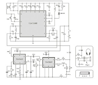
Signal is amplified by audio amplifier dientik two, then reproduced through two speakers are the same. Now listeners can heard coming from the left half the loudspeaker is placed on the left and right half of which is placed on the right side. Situation amid the orchestra will be equal to that of the second lordspeaker reproduced, made an impression on the listener as if there.
The third loudspeaker placed midway between the left and right. Based on all these listeners have a picture of the layout space, which is significantly increased total musical impression. Electronic circuits of the portable stereophonic radio receiver with headphones reproduction, made by the IC TDA 7088T is shown in Figure the above. This is a practical embodiment of the receiver with TDA7040T decoder and two audio amplifier with TDA7050T IC.
Choke (coils) L3, L4 and L5 are HF coil allows the headphone cable is used as a receiving antenna. this fulfilled by connecting one contact of the plug-in headphones, through a 10 pF capacitor at the point where the output of the antenna is connected. Coil has a significant barrier to the signal station, preventing ground connection through capacitor 47 mF or through the TDA7050T output.
Thursday, November 14, 2013
Multiplexer Circuit With Logic Gate
Multiplexer circuit with a logic gate is a multiplexer circuit that utilizes a combination of logic gates.
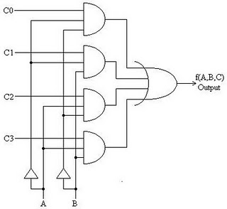
The working principle of the multiplexer circuit above is:
1. Value of bit 00 from the selector will choose the path of the first input as the output
2. Value of bit 01 of the selector will choose the path of the second input as output
3. Value of bit 10 of the selector selects the third input lines as output
4. Value of bit 11 of the selector will choose the four input channels as output
5. As long as there is no change in the bit selector logic condition of the output logic state also will not be amended.
6. If the line selector is connected with a series of counter-up the output to be obtained will represent the input lines in sequence.
7. So it can be concluded that the usefulness of the implementation of a multiplexer function is to satisfy the principle of a simple data distribution. Thus, with multiplexers is possible to transmit data remotely using only one connection.
Read More..
Where the above example can be seen that the circuit has 2 bit selector and 4 input lines. You can make a circuit with more input channels by increasing the number of bits of the selector. And also you can use a combination of gates based on your own design with reference to the previous multiplexer truth table you should specify. So by making a truth table in advance you can easily create a series of logic gates.
The working principle of the multiplexer circuit above is:
1. Value of bit 00 from the selector will choose the path of the first input as the output
2. Value of bit 01 of the selector will choose the path of the second input as output
3. Value of bit 10 of the selector selects the third input lines as output
4. Value of bit 11 of the selector will choose the four input channels as output
5. As long as there is no change in the bit selector logic condition of the output logic state also will not be amended.
6. If the line selector is connected with a series of counter-up the output to be obtained will represent the input lines in sequence.
7. So it can be concluded that the usefulness of the implementation of a multiplexer function is to satisfy the principle of a simple data distribution. Thus, with multiplexers is possible to transmit data remotely using only one connection.
Wednesday, November 13, 2013
MPC576H Amplifier Circuit Diagrams
This amplifier circuit has a pretty good quality. Of course the sound quality, although this one amplifier does not have a large output power but in terms of soft and loud voice that this amplifier can be unreliable. With a single IC capitalize MPC576H and several other supporting components you have to make this amplifier circuit. Voltage at least 9 Volt and 24 Volt Max. Output Power 3.5 Watts with 8 Ohm impedance.
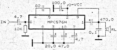
| MPC576H Amplifier Circuit Diagrams |
Tuesday, November 12, 2013
USB Soundcard Circuit with PCM2702

You do not need to install drivers for Windows XP and Vista, because the driver is already in the system, XP and Vista. So this series is really plug and play.
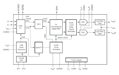 |
| Block Diagram |
Description
The core of this construction is a 16-Bit Stereo Digital-To-Analog Converter with PCM2702 USB interface.
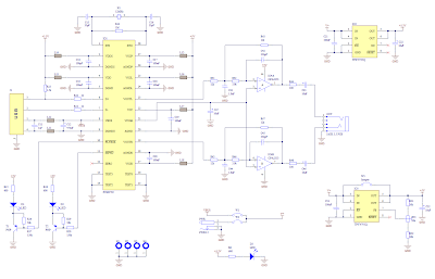 |
| Schematic diagram USB soundcard |
PCM2702 only requires a few additional components to work. This scheme is not complex. The sound card can be activated directly from the USB port (jumper W1) or from an external power supply (jumper W3). PCM2702 requires two 3.3V power supply (3V-3.6V) and 5V (4.5V-5.5V). I use a fixed output voltage to 3.3V LDO TPS76733Q (IO2) and the output voltage is adjusted to 5V LDO TPS76701Q (IO3).
LDO Both are produced by TI, I use it because there in my drawer. Each LDO The same can be used. IO3 output voltage should be set to slightly lower than the input voltage to enable LDO stabilization is good, in my case the output voltage set to 4.8V. output voltage can be set by the resistor R33 is adjusted. In the case of low power supply, IO3 be shorted by the W3 jumper. Signalizes D3 LED power on.
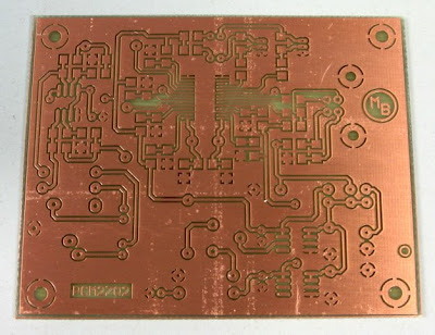 |
| PCB line design usb soundcard |
 |
| Layout PCB usb soundcard |
Small ferrite beads are placed before all power pins on the PCM2702 and GND Vbus and USB. Small beads reduce high frequency hum. I have a problem finding SMD ferrite beads small local shops but finally I get some of them from the old hard drive. They are not really necessary, you can use zero ohm resistors instead of them.
Low-pass filter placed in the output signal path to reduce the sampling frequency. OPA2353UA dual op amp configured as two stereo-order low-pass filter. Led diodes D1 illuminates when the PCM2702 play audio data received from the USB bus. Diode D2 Led illuminates when the USB bus audio delay the transmission of data to the PCM2702.
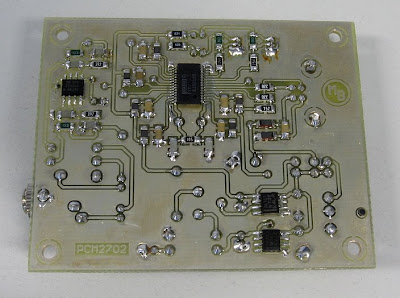 |
| Installed component USB soundcard |
This circuit works very well. I just had shorted crystal during soldering so that circuit does not work, but after removing the short noise, a sound card to work. I have been tested on Windows 2000, XP and Vista. The electronic circuit works in all the systems mentioned. Driver is in the operating system so that the sound card is ready within a few seconds after you connect the electronic circuit is with a PC / Laptop / Notebook you are in trouble with the sound card / sound card that.
During writing this article I have found that the PCM2702 is now not recommended for new designs, but TI offers a better solution. PCM2704, PCM2705 has the same functions as the PCM2702, but they include an output filter. They were able to push the headphones directly.
Volume and mute can be controlled via the SPI bus in PCM2705 or PCM2704 with pushbuttons in the case. PCM2704 and PCM2705 are in TSSOP28 package. PCM2706 PCM2704 and PCM2707 similar to PCM2705 but in addition they have the I2S bus. PCM2706 and PCM2707 are in a TQFP32 package. I recommend using the new chip (PCM2704 / PCM2705) for the new design an Operating System.
Monday, November 11, 2013
150 watts power amplifier circuit
Amplifier circuit is 150 watts power amplifier circuit is quite simple.
This circuit requires only 5 pieces of transistors as the main component of reinforcement. There is no equalizer option on this amplifier circuit because it can be said of this series is very simple, so do not you compare it with that sold in the market which are usually equipped with various sound system and equalizer settings.
This circuit requires only 5 pieces of transistors as the main component of reinforcement. There is no equalizer option on this amplifier circuit because it can be said of this series is very simple, so do not you compare it with that sold in the market which are usually equipped with various sound system and equalizer settings.
But to add to your collection circuit, this circuit is fairly easy and inexpensive to make and maybe one day you may need as a weak signal booster from your electronic circuit. Or you can also make this amplifier as an amplifier of high frequency signal from the output circuit animal repellent and I guarantee the results are very satisfactory.

Power supply required is two-polarity power supply is + - 45 volts. Maximum power that can be obtained by this amplifier circuit is around 150 watts. As the volume control you can add potensio or variable resistor 10 Kohm in series at the input. Use dispasi loudspeaker with 150 watts power. Use a heatsink on the transistor-transistor driver loudspeaker or amplifier late as Q1 and Q2.
Sunday, November 10, 2013
Portable Battery Charger Circuit
This circuit was designed to charge Nicad battery packs in the range of 4.8 to 15.6 V from a convenient remote power source , such as automobile battery. When power is first applied to the circuit applied to the circuit , a small bias current supplied by R1 via winding L1 , starts to turn on the transistor TR1.This forces a voltage across L2 and the positive feedback given by the coupling of L1 and L2 causes the transistor to turn hard on , applying the full supply across L2. The base drive voltage induced across L1 makes the junction the necessary base current to hold Q1 on.

Resistor
R1 = 1M
R2 = 120R
R3 = 10R
R4 = 39R
Capacitor
C1 = 100uF 25V
C2 = 0.01uF
C3 = 4700pF
C4 = 100uF 25V
Diode
D1 = 1N4148
D2 = BYV27-5
D3 = BYV27-5
Transistor
Q1 = ZTX650
Transformer
L1 = 12T 36awg
L2 = 13T 36awg
L3 = 20T 30awg
L4 = 40T 30awg
Core FX3437 with gap of 0.08mm
Former DT2492
Saturday, November 9, 2013
USB FX2 USB 2 0 interface board circuit schematic
 USB-FX2 USB-2.0 interface board circuit schematic
There are some things one should be aware of when building the design above:
- Resonator: According to the data sheet, the FX2LP has an on-chip oscillator circuit which requires an external 24MHz (±100ppm) parallel resonant, fundamental mode crystal with 500uW drive level and 12pF (5% tolerance) load capacitors. So, you cant just put any 24MHz crystal there but things dont seem to be as critical as one may expect. Im using a 24MHz fundamental mode crystal (24-MA505 from Reichelt) with 10..15pF caps (or even 32pF).
(Note: In the schematic above, there are 2 crystal oscillators in parallel merely to have both options on the PCB (one of them is an SMD). Only one of them is actually soldered onto the board.) - EEPROM: You can use an optional serial EEPROM to store either USB configuration data or a complete program which is loaded into the microcontrollers RAM at startup. You can leave it away completely to use default USB config data and download firmware via the USB (thereby also changing, the config data, its the so-called ReNumeration thingy). Note, however, that if you leave away the EEPROM, you must still put in both the 2.2k I2C bus pull-up resistors.
- PWR_SEL: For USB-powered operation (500mA max), close a jumper between pins 2 and 3, for externally powered operation, apply 5V and GND to pins 2 and 1, respectively. There is an additional 5V, 3.3V and GND power connector called PWR_HUB to connect with add-on boards.
- For 5V-to-3.3V conversion, you need to use an LDO (low-dropout regulator) like the LM2937. It should have a drop-out of 1.2V max since the USB specs allow the 5V voltage to be as low as 4.5V on the slave side.
- Of course, usual voodoo applies like putting decoupling caps near by and keeping the USB data lines short. A massive ground plane is mandatory, at least for the analog half. Forget about Cypress telling you that you need at least a 4-layer PCB. My regular 2-layer PCB (ground plane on bottom) works stable in high-speed mode even with 3m USB cable.
Friday, November 8, 2013
HiFi Amplifier circuit schematic
This is HiFi amplifier use the IC TDA1111 . The circuit is quite easy to use, but the constraints on the IC is difficult to find my local region. If you have this IC , it is very suitable is made by this circuit. Minimum voltage on the circuit 6-Volt and a maximum of 20 volts. And voltage suitable for supply of 12 Volt. Maximum power output of 40 Watts with 4 ohms impedance, and frequncy of about 20Hz to 20kHz. See the circuit below :

Thursday, November 7, 2013
Mosfet Snubber Flyback Converter Circuit
Mosfet Snubber Circuit in Flyback Converter , Typical flyback convertor with drain clamping circuits ZenBlock Zener with integrated blocking diode Philips Semiconductors new ZenBlockTM replaces double-diode-, RCD- or RC-snubbers in flyback convertors.
 |
| Mosfet Snubber Flyback Converter Circuit |
The new components offer circuit designers the important benefits of lower component count and board usage, reduced EMI, optimal clamping at all loads and higher efficiency. Introducing The new ZenBlock combines the double diode snubber in one package. This leads to the following advantages:
-Fewer components.
-Reduced circuit board space
-Lower EMI by reducing the drain clamp circuit length and area.
-Optimal clamp performance at all loads (compared with RCD and RC snubber)
-Higher efficiency at low loads (compared with RCD and RC snubber) . Previous circuit related to this circuit : Protection of the Mosfet in flyback power supply
FM Radio Receiver Circuit with IC TDA 7012T
TDA 7012T FM Radio Receiver
FM Radio Receiver IC TDA 7012T is very simple, but it has an FM radio receiver sensitivity and good selectivity. Single Chip FM Receifer cool name of IC TDA7012T 7012T TDA is to build an FM receiver requires a few additional components.
Feature contained in FM receiver IC TDA 7012T is quite tempting to an FM receiver. Among features an FM receiver TDA 7012T is a low-voltage applications micro affability arrangement (MTS), Frequency Loked Loop (FLL) to 76 KHz range and selectivity of FM receiver with RC Filter. In an article by FM Radio Receiver IC TDA 7012T can be seen in the FM receiver circuit which can be made.
FM Radio Receiver with IC TDA 7012T
From the picture above components to make the FM Radio Receiver IC TDA 7012T as follows:
R1 = 8kΩ2
R2 = 10kΩ
R3 = 390Ω
C1, C3 = 10nF
C2, C6, C9, C16 = 100nF
C4 = 33pF
C5 = 25pF trimmer
C7, C10 = 1nF5
C8 = 820pF C11 = 1NF
C12 = 68pF
C13 = 220pF
C14 = 47μF 10V
C15 = 3nF3
L1 = 36nH
L2 = 1μH,
IC1 = TDA7021T
Hopefully useful and become an idea in the manufacture of Mini FM Receiver with IC TDA 7012T
Tuesday, November 5, 2013
AN5265 Amplifier Circuit
Schematic Description :
This Circuit Require voltage 12 -26 Volt. Good Voltage use is 16 Volt , Because its not too small and not too big Voltage. If use voltage that is to large it will quickly damage the IC. And if use voltage that is to small it will make less than maximum sound output.
See this Circuit and datsheet IC AN5265 Below :
 |
| Click to Enlarge |
Datasheet IC AN5265
Vcc = 12-26 V
Pout = 2,3 W
RL = 16 Ohm
Ft = 40hz - 18Khz
Icco = 9,5mA
Package = SIP2-9
Manufactered = MATSUSHITA
Saturday, November 2, 2013
Power Amplifier Circuit for Computers
At this point is a minimal / simple power amplifier on behalf of boosting the audio level from low-power Computer sound cards before other audio sources driving tiny speakers like toys otherwise small transistor radios. The circuit pray set free around 2 watts to the same degree given away. The parts are not significant and substitutions will commonly job. The two 2.2 ohm resistors might live replaced with solitary 3.9 ohm resistor featuring in either emitter.
 |
| Power Amplifier Circuit for Computers |
Friday, November 1, 2013
DC fan control circuit for power amplifier
DC fan control circuit for power amplifier .Variable speed DC fan This series of works based on the input signal. Speed / fan rotation depending on size of the input signal coming from speaker lines. If there is no signal then the fan will spin slowly according to the setting VR1. Input supply can be taken directly from the main transformer power amplifier, 12V CT 12V, so no need to increase the transformer again.
This circuit has been tested and do not cause buzzing. correction: the lowest R: 560 ohm
 |
| Circuit Schematic Electronics | CSE |
This circuit has been tested and do not cause buzzing. correction: the lowest R: 560 ohm
Wednesday, October 30, 2013
Simple accu charger circuit

Accu charger circuit is very simple and easy to make, because it only requires a few components are also not more than 10 components. Besides easy charger circuit is also very cheap and very efficient.
This circuit requires power supply from a transformer that comes from an AC voltage 220 and diuturunkan be 12-13 volts and then enter to-circuit and 12 Volt DC output allows for charging 12V battery
| Simple charger schematics |
Tuesday, October 29, 2013
50W AF Power Amplifier with STK4036II Schematic Circuit
 50W AF Power Amplifier with STK4036II Schematic Circuit
• Compact package for thin-type audio sets
• Member of pin-compatible series with outputs of 20 to 200W
• Easy heatsink design to disperse heat generated in thintype stereo sets
• Constant-current circuit to reduce supply switch-on and switch-off shock noise• External supply switch-on and switch-off shock noise muting, load short-circuit protection, thermal shutdown and other circuits can be tailor-designed.
Monday, October 28, 2013
Flip Flop Led Circuit
Flip Flop LED
Flip flop circuit is a series of free runing multivibrator given the burden of LEDs on each side of the transition changes its output signal. Flip flop circuit with LEDs is quite simple, that is prepared with 2 units and 2 units of 2N3904 transistor circuit tank circuit composed by the RC circuit.
LED indicators signal a change that is placed on each side of the flip flop will be lit in turn by the fire and extinguished the same as the charge and discharge capacitor. Flip flop circuit is quite simple as shown in the picture below.Flip Flop LED series

The working principle is the flip flop over when the series voltage source is given then the 10uF capacitor will be charged through R 470 and the LED will then be forwarded to triger the transistor base so that the transistor will turn ON and LEDs. this occurs alternately on each side, so that the LED light will illuminate in turn as well.
Subscribe to:
Posts (Atom)